Digital isolators are a modern replacement for optocouplers: components that can bring a signal from one place to another without connecting those two places electrically. They’re essential parts in equipment that connects to a dangerous voltage on one end (mains power usually) and comes into close contact with something sensitive on the other (humans, usually). Since they’re safety-critical components, manufacturers show off all kinds of safety certificates and qualifications to convince their customers that their isolators won’t electrocute anyone by mistake.
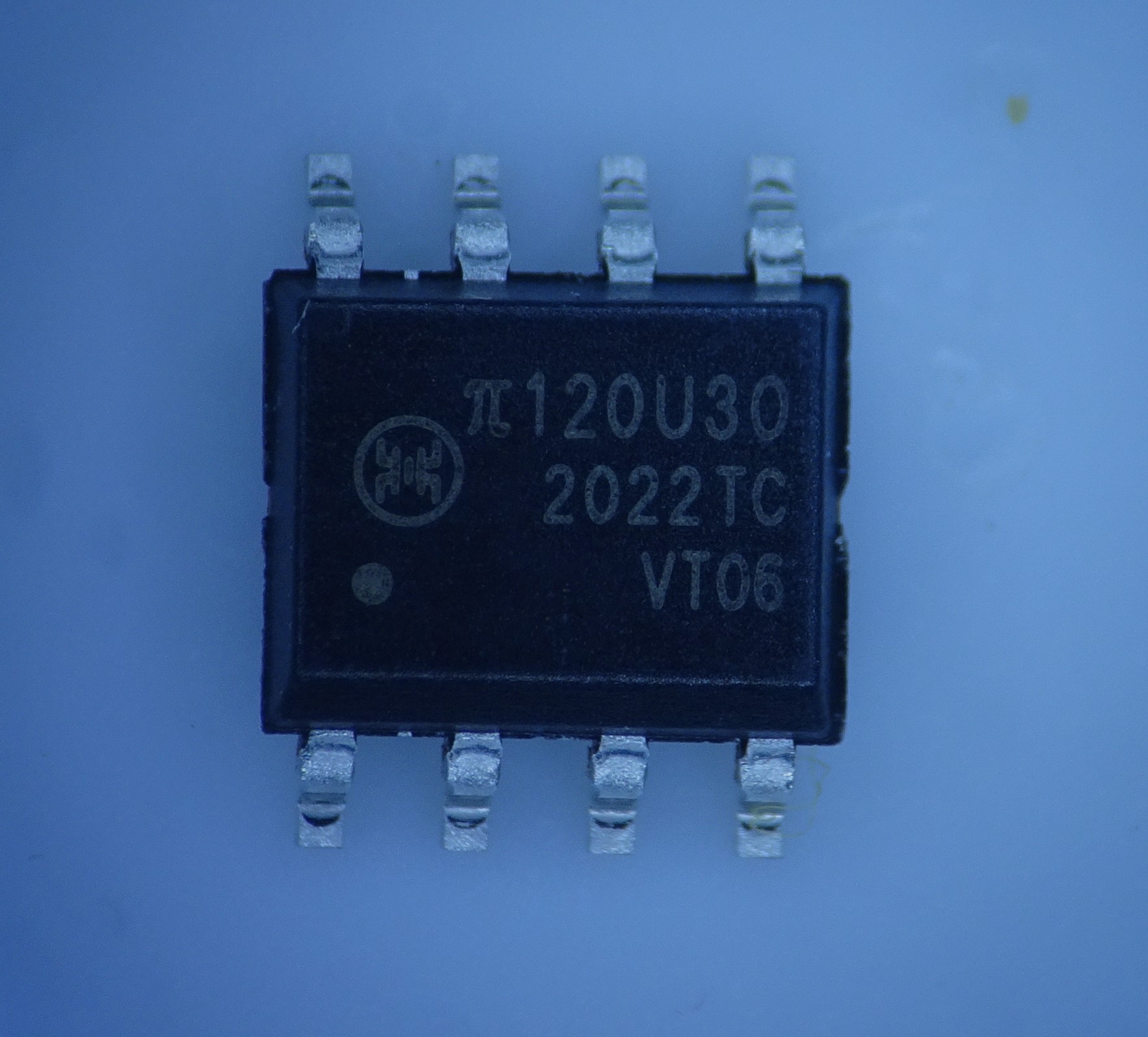
Today we’ll look at one of the cheapest digital isolators out there: the π120u30, made by 2Pai semiconductor, which costs less than 20 cents in large quantities.
2Pai semiconductor, a relatively new manufacturer based in Shanghai, appears to specialize in digital isolator chips. They have quite a large selection, mostly variations of the same basic design with different numbers of inputs and outputs, various packages and multiple isolation levels. The 120U30 has two inputs on one side and two outputs on the other. You can get similar chips with one input and one output on each side.
The chip is rather simple to use: pins 1 to 4 (the bottom row in the picture) are the two inputs, with their own supply and ground pins, while pins 5 to 8 are the output, also with their own supply and ground. Any digital signal you apply on the input will be replicated on the output.
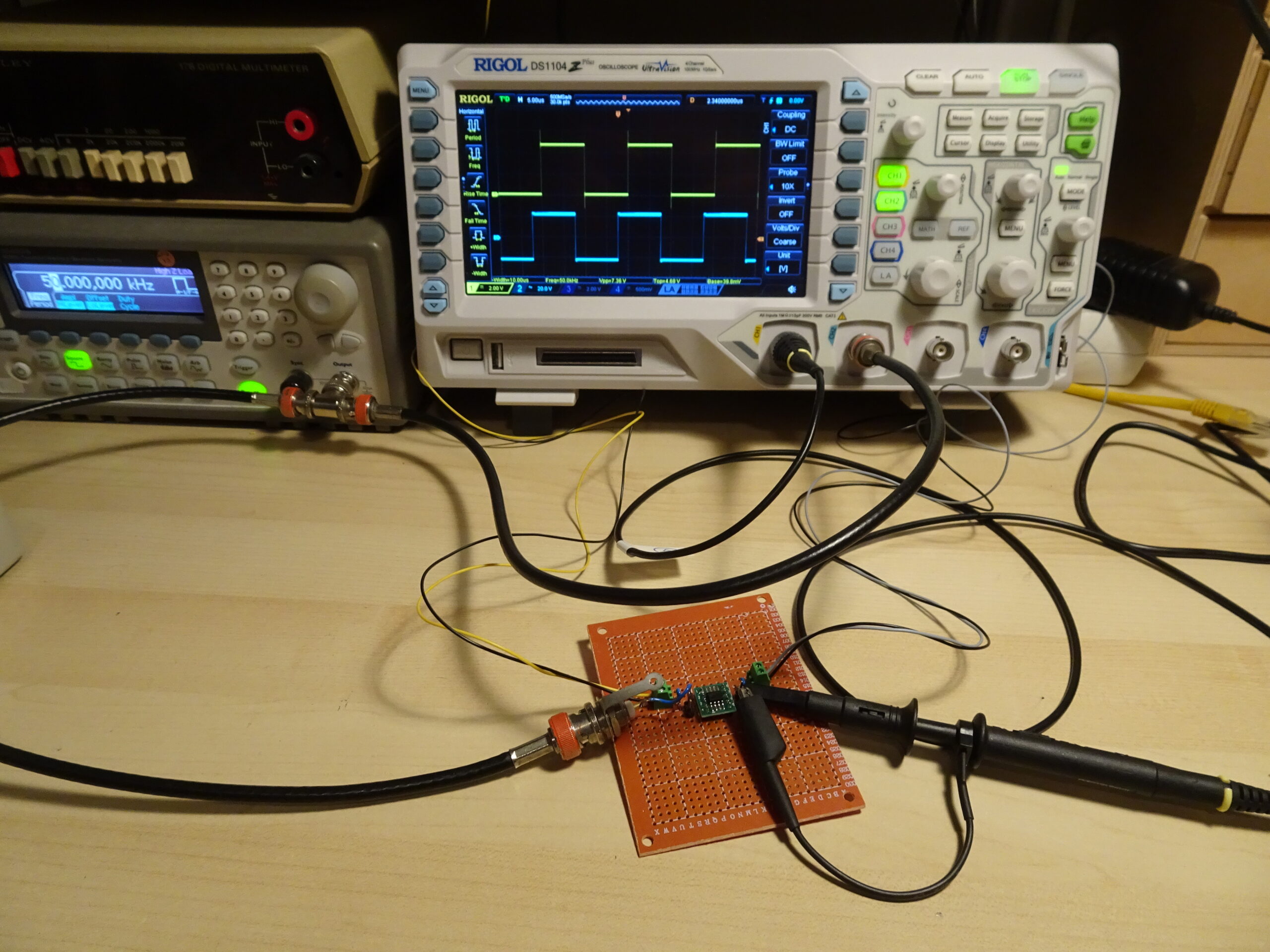
I made a little test board to try out the basic functionality. As expected, the input (in blue) is simply replicated on the output (in yellow), with a delay of about 2 μs. Both supplies can be anywhere between 3.3 V and 5.5 V, and the chip will withstand 3000 V between the two sides for at least one minute. I didn’t test that last claim, but it’s quite amazing that this is possible in such a tiny 4 mm x 5 mm SOIC package.
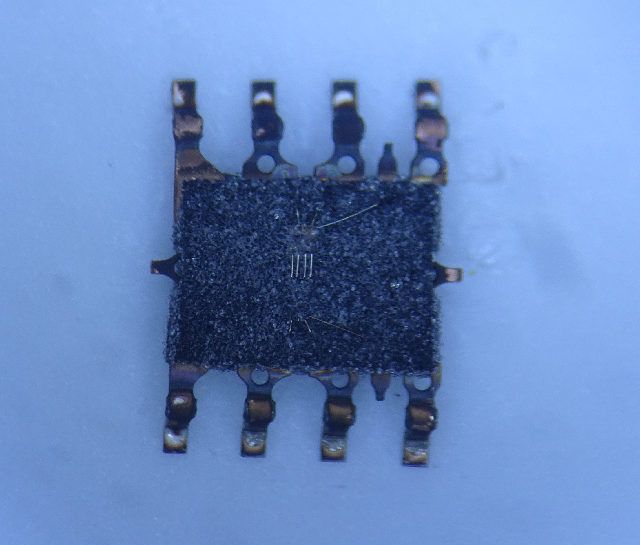
If we partially remove the package, we can clearly see that there are two separate chips inside, connected to each other by four bond wires (the vertical ones in the middle). The way this isolator works is through capacitive coupling: high-voltage capacitors on the chips provide insulation from high voltages, but allow low-voltage signals, modulated at some carrier frequency, to pass through. Both sides of the device need circuitry to modulate and demodulate the signals; this is why there are two separate chips in this package, because it’s not possible to provide very strong insulation between components on one chip.
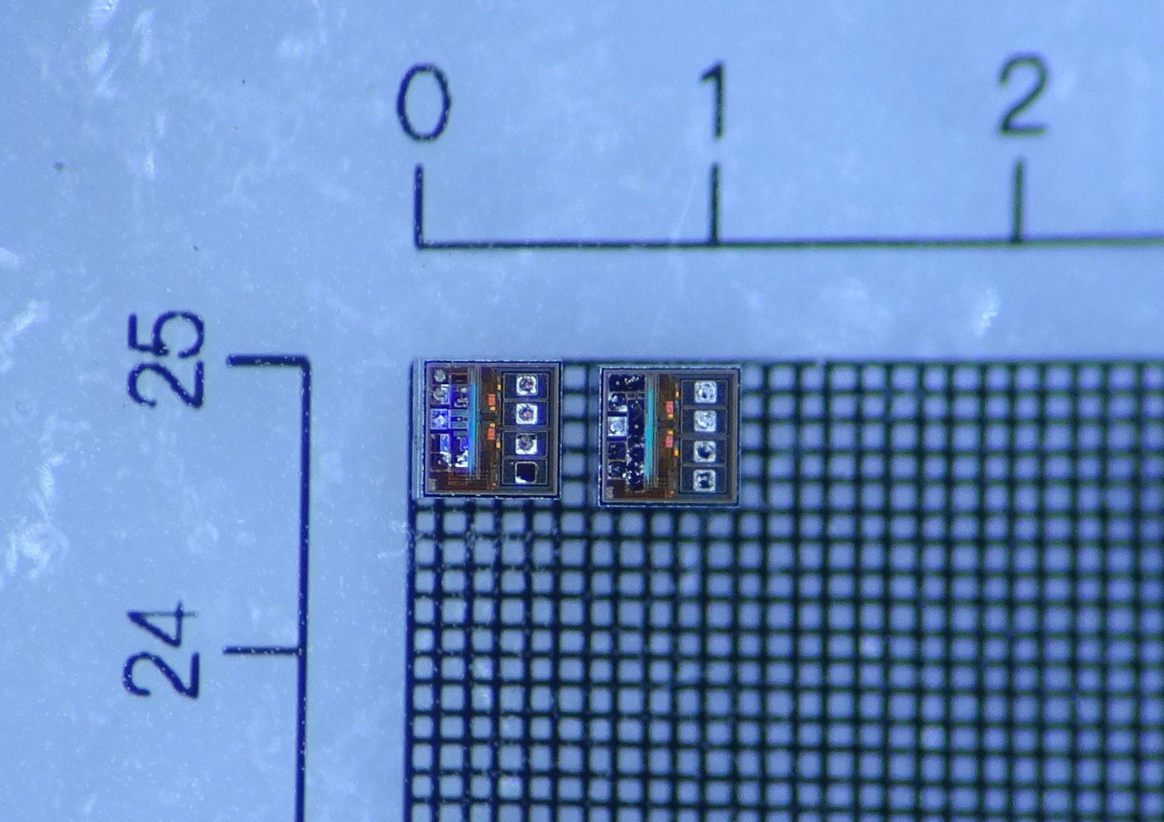
After removing all the plastic we’re left with these two chips. What’s interesting is that they appear to be identical: it’s probably more economical to manufacture just one type of chip that can work as a transmitter or receiver than to develop two different ones. A very clever trick was used to set each chip to a specific mode, as we’ll find out below. Note also how extremely small these chips are: the scales on the side of this picture are in millimeters, so each chip measures just 0.5 x 0.5 mm2.
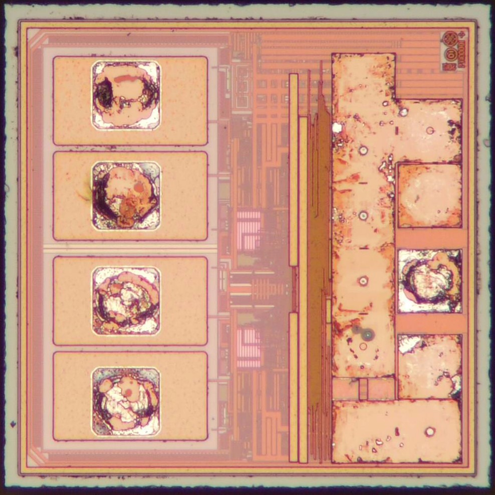
This is a close-up of one of the chips. On the left are four capacitively isolated bond pads, consisting of a layer of metal separated from the layers below by a layer of thick oxide. On the right are the regular bond pads that connect to the chip’s external pins.
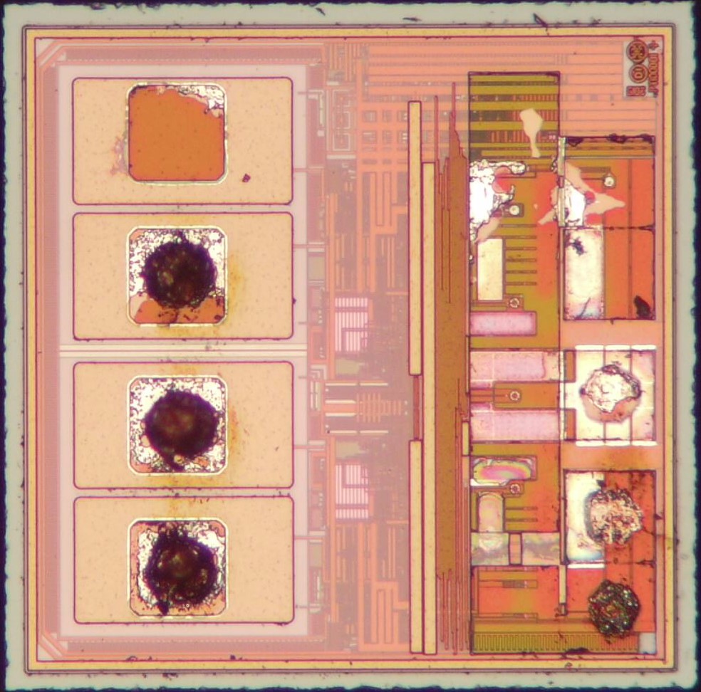
The second chip appears to be fully identical to the first. The bond pads on the right were etched away a bit more than in the first chip, so we can see what’s below them.
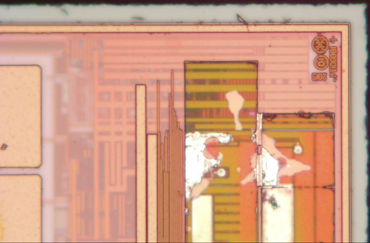
Zooming in a bit, we find a 2019 copyright date, the 2Pai logo and an internal part number PT100001. It looks like there are four metal layers; there might be a special insulation layer below the capacitive bond pads on the left.
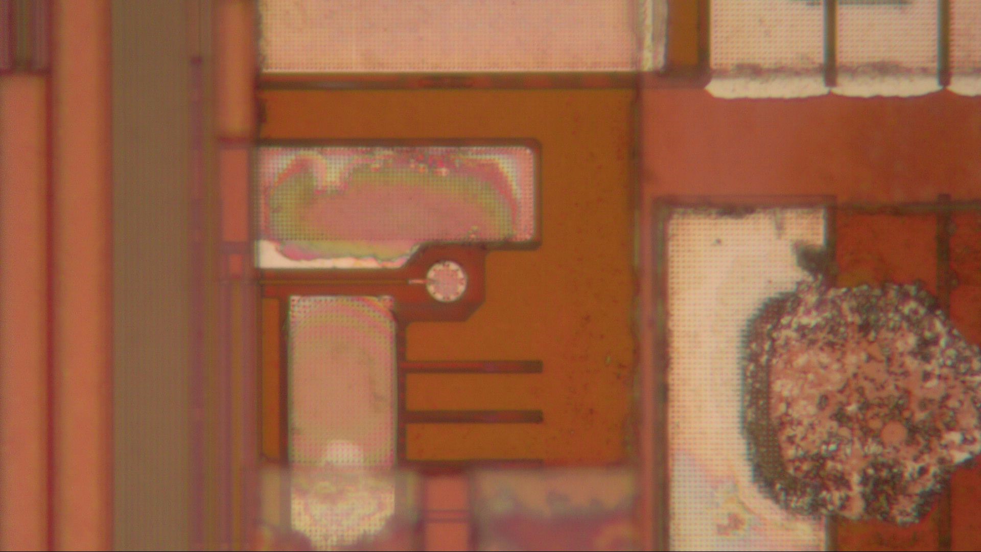
Speaking about bond pads, this is a close-up of what’s below one of the pads on the right. You can see a little round sub-pad in the middle, with a wire leading off to the circuitry on the left. This looks rather odd, so I did some research into 2Pai’s technology and found patents CN110058149 and CN107910309. These describe a method of detecting whether a wire was bonded to a bond pad or not, by having the pad consist of two pieces of metal separated by an insulator. When the wire lands on the pad, it shorts the two together and thereby gives a signal to a detection circuit.
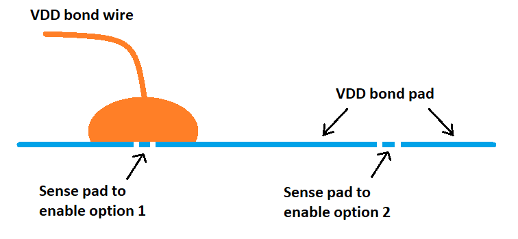
So if we look back at the image of the first chip, there’s one large T-shaped bond pad with little round holes in them. That whole pad is one bond pad (probably either VDD or GND), but depending on where exactly the wire bond is placed, one of the contacts in one of the little holes is shorted to that pin, which is then detected by digital logic to decide which functional mode should be enabled. This is an extremely clever solution, I like it a lot!

If we zoom in onto the lower layers, a very common 3×3 arrangement of square devices is visible: this is a bandgap reference, consisting of nine bipolar transistors. It generates a stable reference voltage that is used for the rest of the analog circuitry.

Down here we find some resistor banks (the pink lines). We can see thick and thin ones, which are connected in several different ways. Overall there’s quite a bit of analog circuitry on this chip, which is needed to generate a stable signal that can pass the capacitive barrier and to demodulate it once it reaches the other side.