A while ago, I found this little PCB in my junk pile:
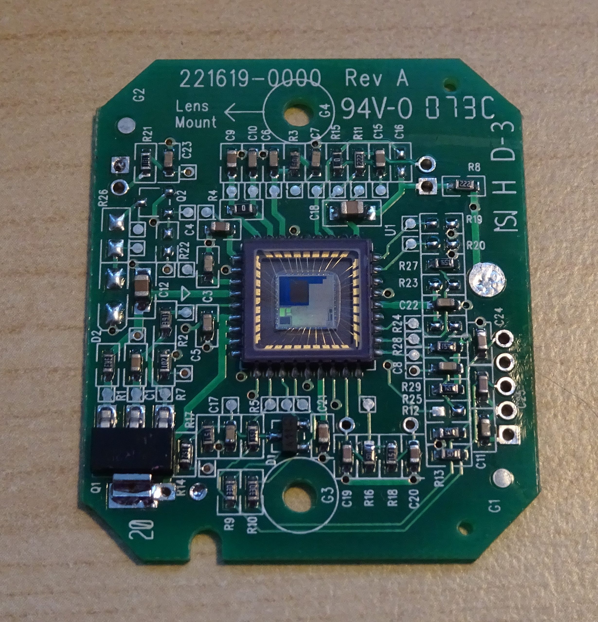
It came out of an old webcam that I used on my PC back in the early 2000’s. Although I didn’t keep any pictures of the webcam itself, I recall that it was a Logitech Quickcam Messenger, a cheap USB camera meant to be used with MSN Messenger and other instant messenging programs. I remember using it for that purpose a few times, but once the novelty wore off it just ended up gathering dust in a corner somewhere.
Many years later, when I needed to use a webcam on my PC for something I tried to use it again, but to my surprise there was no way of getting it to work on Windows 7. I would have thought that this thing would use some generic USB camera driver, but as it turned out it would only work with a custom Logitech driver that didn’t run on anything newer than Windows XP. It ended up on my junk pile, and when I later disassembled it I found that it contains just a single chip, packaged in a ceramic QFN package with a glass cover. This chip contains a CMOS image sensor, readout electronics and a complete USB interface.
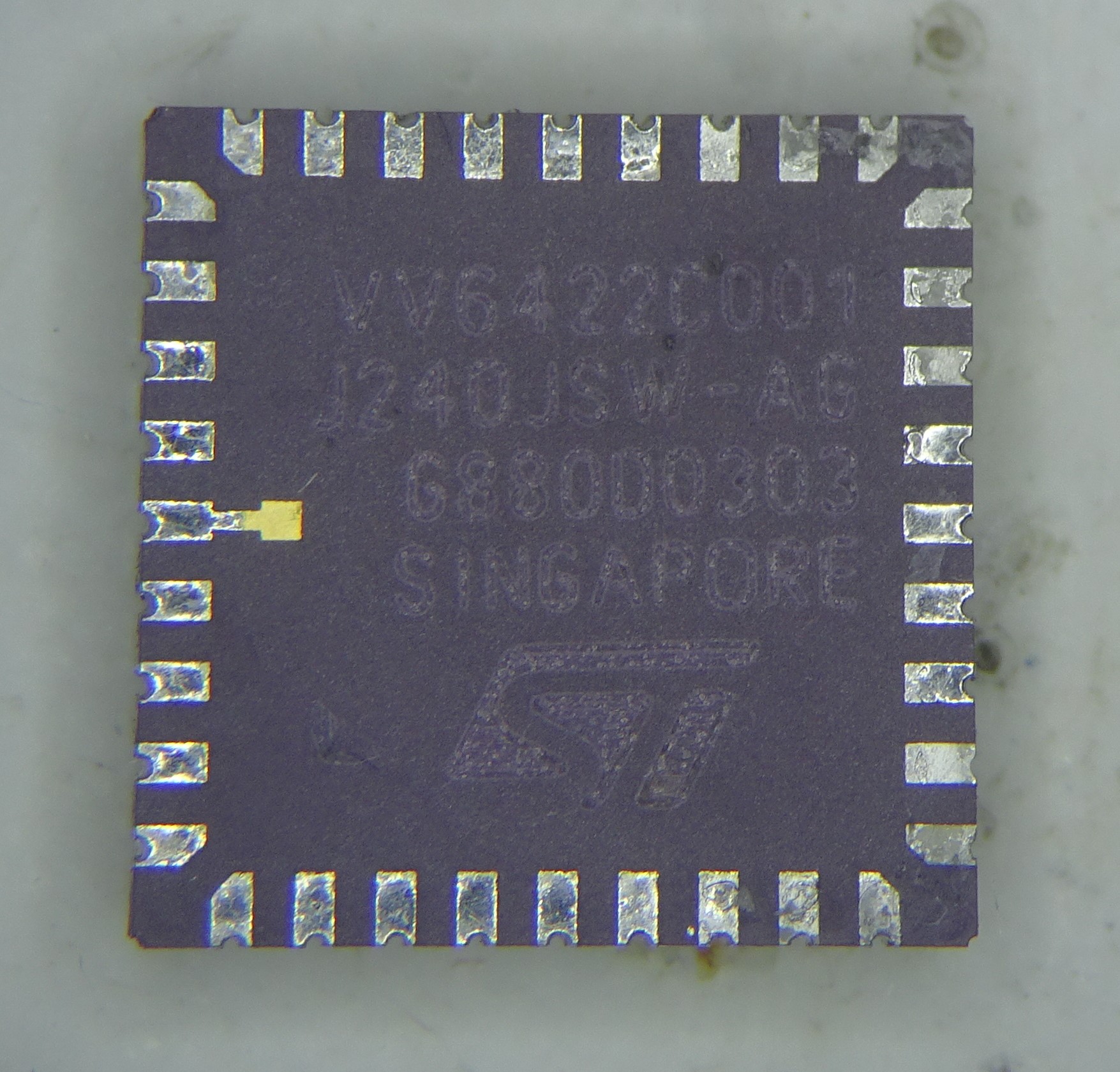
After desoldering we find that it was made by ST. Googling “VV6422C001” gives little information other than distributors claiming to be able to supply it. Most likely it’s simply a custom part made for Logitech by ST.
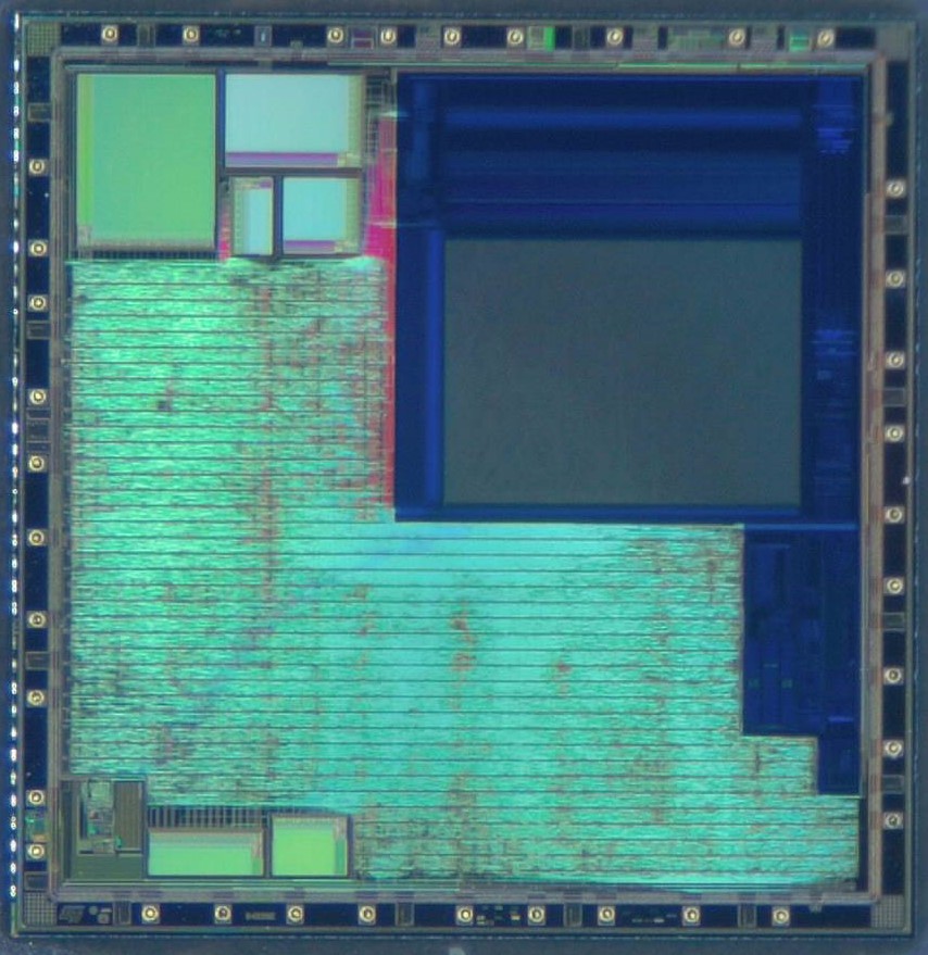
Zooming in on the die, we see several things. The large green area with horizontal stripes is a big block of digital circuits. This implements the USB interface and all digital data processing required. The green/blue blocks on the top left are memory areas, used to store raw data and processed pictures. The grey area slightly above the centre line on the right is the camera sensor: this is where the webcam’s lens focuses the image. The blue area around it contains analog processing circuits that are sensitive to light; the blue layer keeps them in the dark. Finally, on the bottom left are some analog support functions.
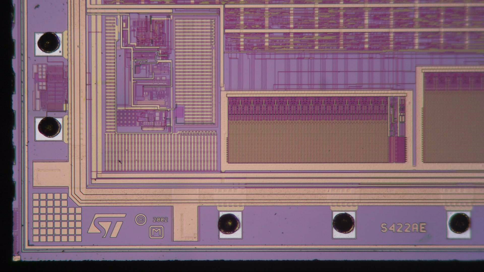
Starting at the bottom, we find the ST logo and a 2002 copyright date.
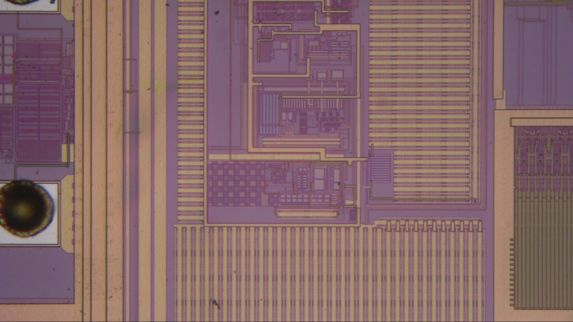
Just above the logo are a few analog support circuits. The bottom section looks like a bandgap reference, judging from the square array of bipolar transistors. The rest likely consists of biasing, timing, startup circuits and so on.
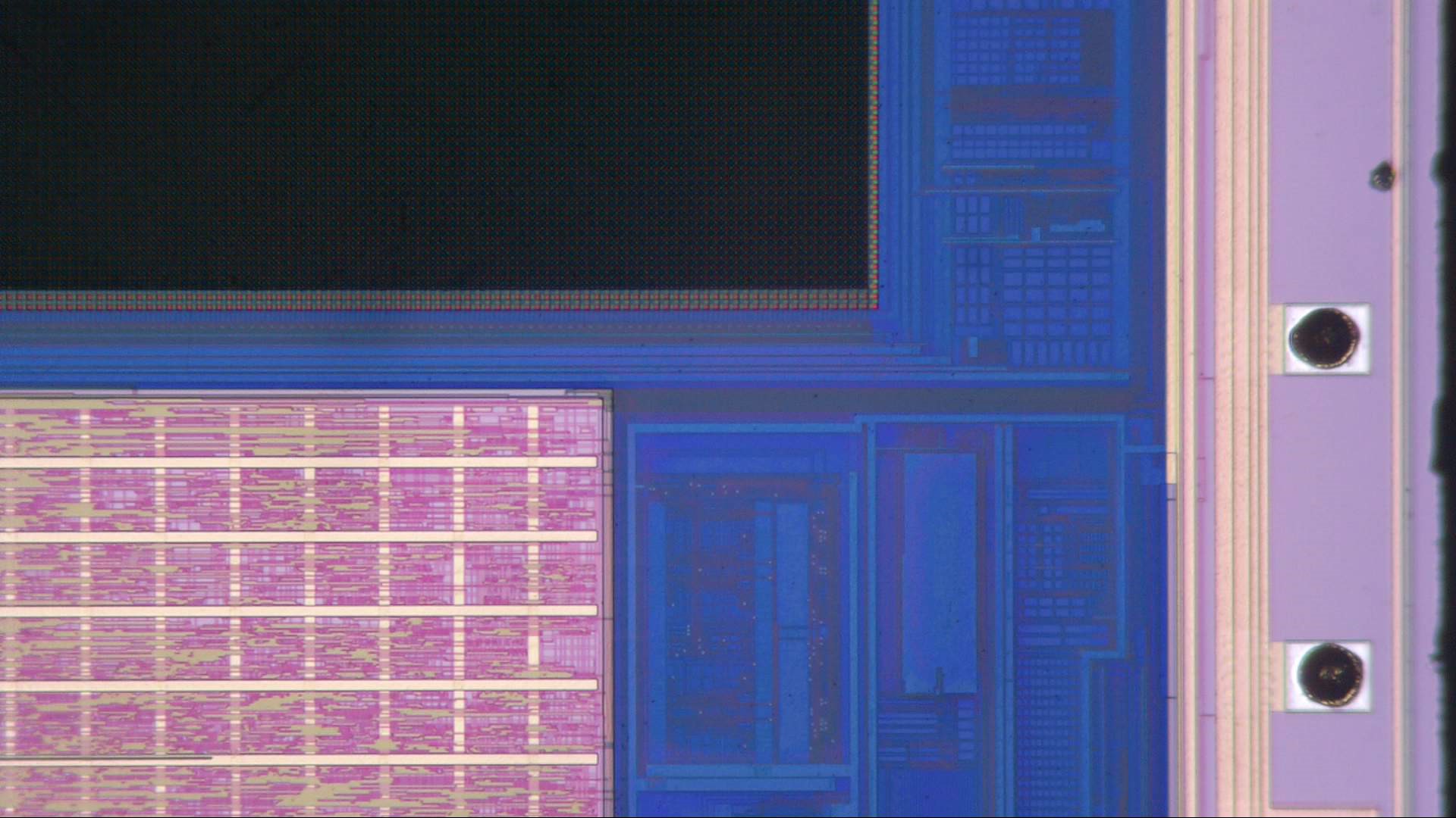
Near the image sensor, lots of circuits are covered by a blue layer. This is to keep them in the dark: if light hits a semiconductor it creates stray currents which can disrupt sensitive (analog) circuits. Digital circuits are not so sensitive, so they are not covered.
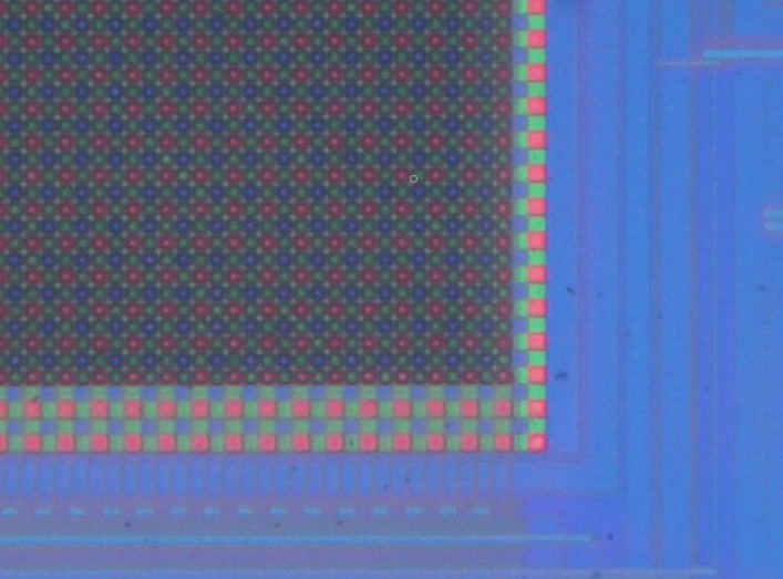
Zoooming in on the image sensor we can clearly see red, green and blue circles. These are a combination of a microlens (which focuses the light on the pixel sensor below) and a light filter, which only transmits a single colour. The pixels are arranged in an array called a Bayer filter, which contains 50% green pixels, along with 25% red and 25% blue pixels. This mimics the response of the human eye, which is most sensitive to green light.
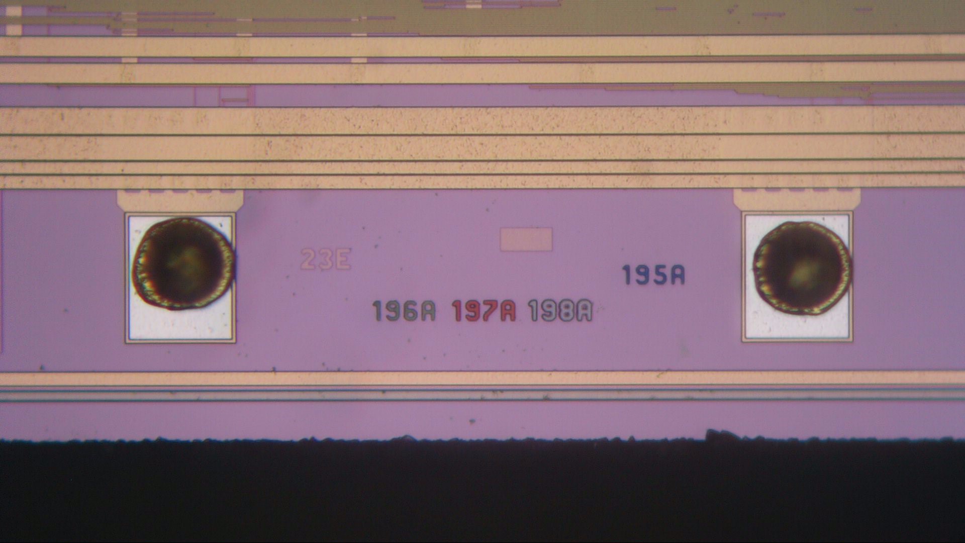
At the bottom edge of the chip we find some layer markers, including the blue, green and red layers. Layer 198 (revision A) might be the layer containing the micro-lenses.