Today we’ll look at another piece of obsolete computer hardware: a Skype handset, officially the “Logitech Cordless Internet Handset for Skype”. It’s a cordless phone that you can hook up to your PC so you can place and receive voice calls over Skype while still holding an actual phone-like device in your hand. I don’t think these things are still popular: in offices you generally find “real” phones, whether connected to an actual phone line or through VoIP, while home users either use a headset for teleconferencing software or their mobile for voice calls.
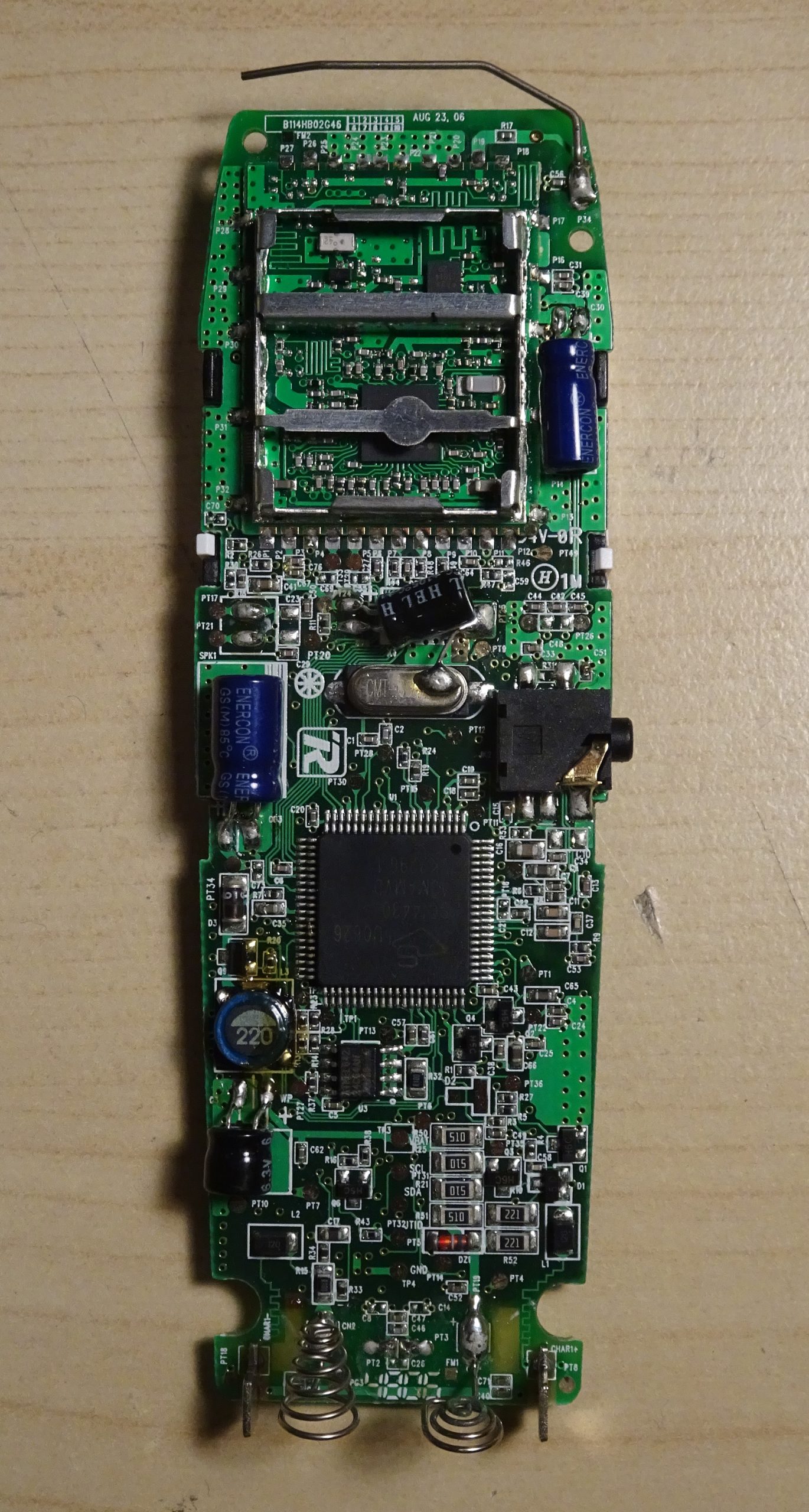
Again, I forgot to take pictures of the complete device, but this is the main PCB found inside. It feels quite cheap, with these radial capacitors soldered horizontally and big blobs of solder on the clock crystal and the battery terminals. It is very well integrated however: all major functionality seems to be packed inside a single IC (the large one in the middle), with two smaller chips implementing the RF interface.
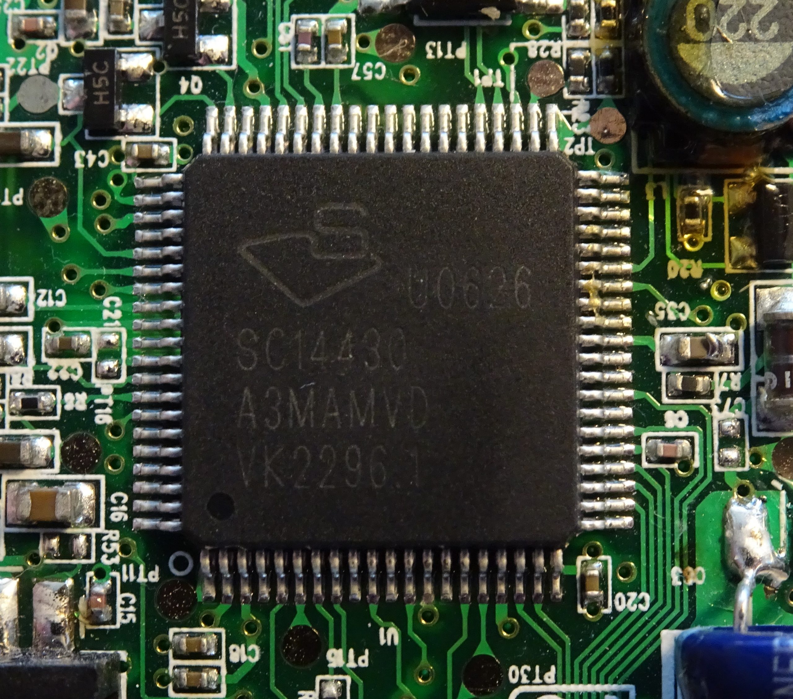
The main chip is an SC14430 made by Sitel. This company has an interesting history: it started as a division of Sierra Semiconductor specializing in DECT chips, and was spun out of that company in the early ’90s. In 1996 it was acquired by National Semiconductor, until it was again spun out in 2005. In 2011 it was acquired again, this time by Dialog, which today still runs Sitel’s engineering team from their former headquarters in the Netherlands.
There’s no documentation available on the SC14430, but it’s likely to be similar to the SC14434 which is commonly used in DECT-enabled internet routers. It probably contains a microcontroller and the essential baseband processing needed to implement the DECT protocol. After all, this is really just a DECT phone, although connecting to a base station plugged into a computer rather than into a phone line.

After removing a metal shield we find two chips powering the RF section: one made by Sitel again, labelled LMX4169, and another with just the numbers 624, 1914 and 29. We also see lots of external components and some PCB stripline circuits.
The LMX4169 part number provides a hint towards Sitel’s National heritage: National Semiconductor’s part names generally start with LM (Linear Monolithic, meaning “analog IC”), then a letter indicating the general function (X for RF parts), followed by a number to identify the part.
The smaller chip is probably a power amplifier, given its location near the antenna. Both chips are packaged in tiny QFN packages.

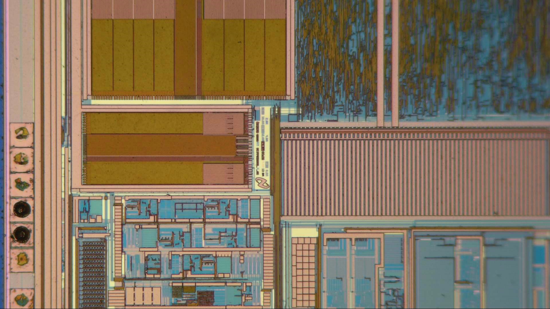
Here we’re looking at the big IC, the SC14430. On the lower right there’s a huge memory area, storing the microcontroller’s main program code. At the top left we see some memory cells, with most of the remaining area used by digital circuits. On the lower left are some analog circuits.
Zooming in, we find the National Semiconductor logo. Sitel is nowhere to be seen; this chip must have been designed before the company became independent.
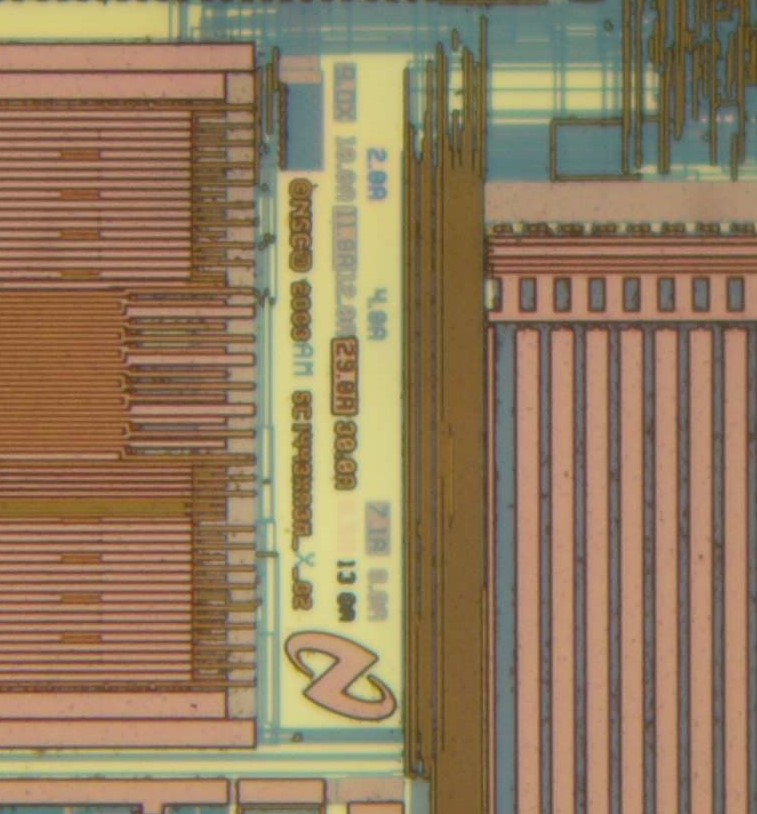
The logo area shows a 2003 copyright date, which was well before the Sitel spin-out. Also, the part number is identified as “SC1443X”, suggesting that it’s part of a family of similar parts including the SC14434. An online search confirms that this is the case, and that these chips contain a 16 bit microprocessor (based on the CompactRISC architecture from National) and an integrated DSP.
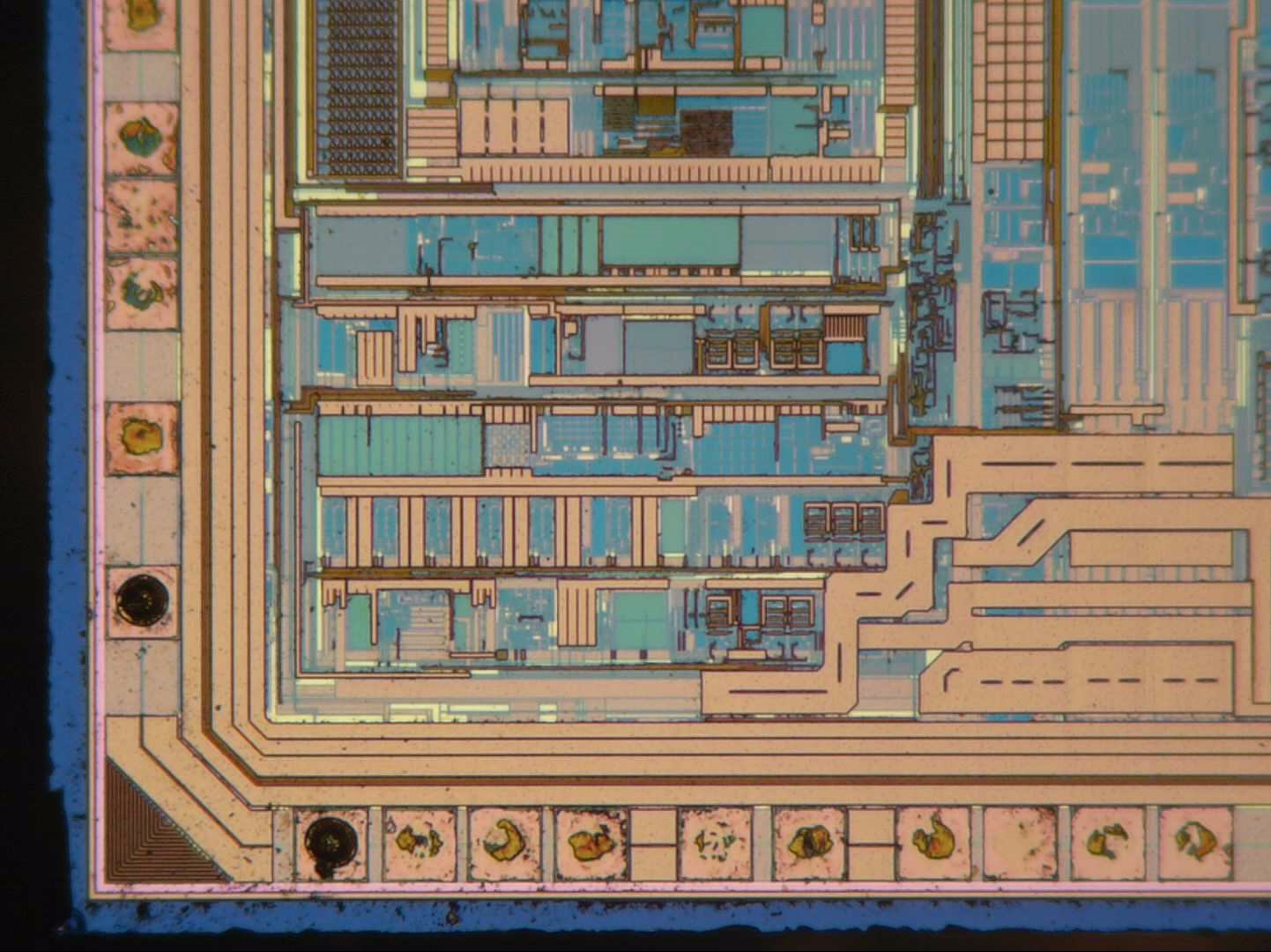
In the bottom-right corner are many analog circuit blocks. It doesn’t look like much RF work is going on here: this IC generates baseband signals which are mixed up to the carrier frequency (around 1.9 GHz) by the smaller chip.
At the top edge of the chip are these bond pads. The fact that two or three wires are used for a single signal usually means you’re looking at pads for the supply voltage, but in this case it looks like these are RF pads. These may use multiple bond wires to lower the inductance and thereby decrease signal loss at high frequencies. The circuit with the little square blocks just below the bond pads look like RF circuits, with their symmetrical layout.
Now let’s look at the second chip, the LMX4169. This is an RF IC: the large inductor at the top is a clear sign of that. There is also some digital processing in the centre and at the top right. No information is available on this chip either, but there is a datasheet floating around the Net describing a similar chip, the LMX4168 (although not in much detail). Based on that datasheet, we’re looking at a complete DECT transceiver with an LNA, mixer, PA driver and VCO, made in National’s 0.25 micron process.
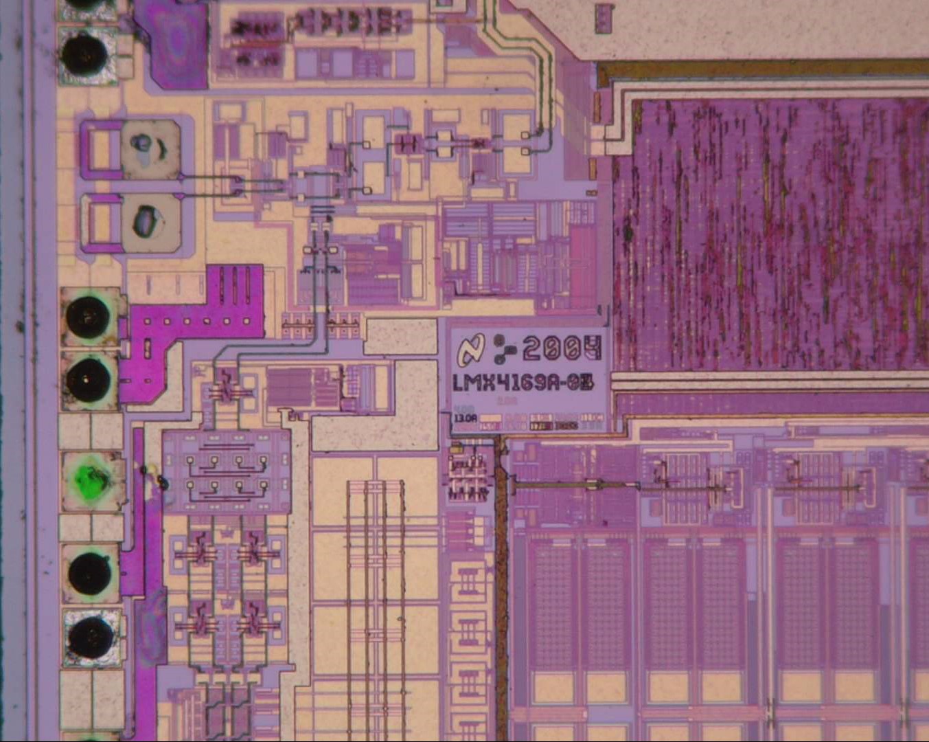
Inside, we find a 2003/2004 copyright date. Apparently the first version was released in 2003, represented in the lower layers of the chip, and some update was performed on the top metal layer, where the “3” was replaced with a “4”.On the left we can see the RF signal path: differential lines coming in from the two pads, probably entering a mixer, with the VCO on top and the rest of the signal path going down the left side.
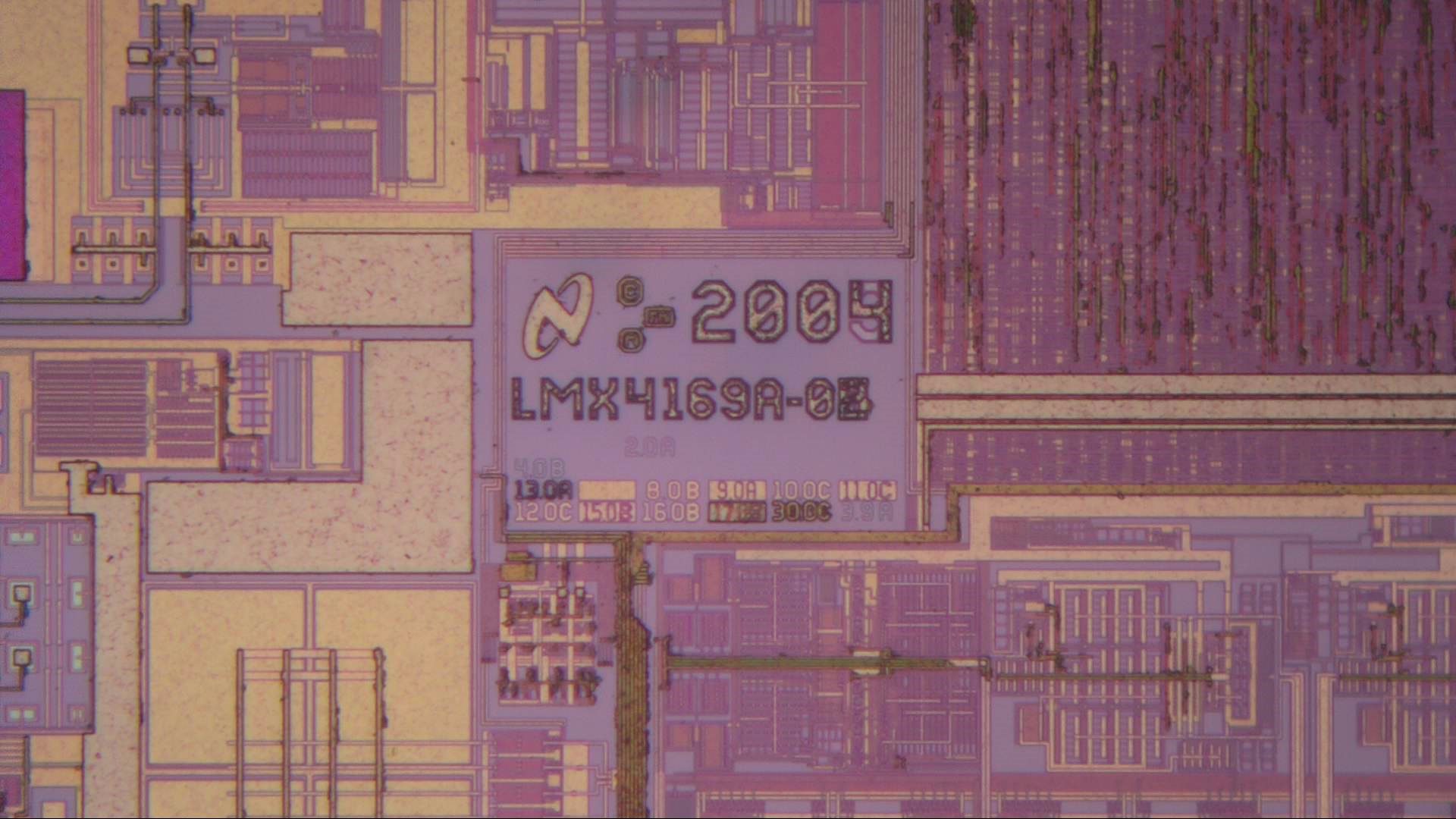
Looking a bit closer we can see the mask identifiers. We can see that layer 8 is at revision B, layer 9 is at revision A, and so on. This chip is made with five metal layers.
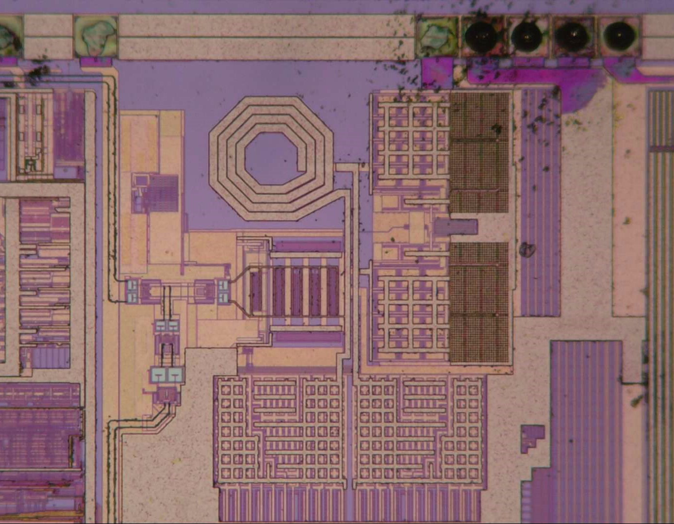
Here we see the VCO (Voltage Controlled Oscillator), which generates a high-frequency signal to mix signals up and down between baseband and RF. The octagonal inductor determines the frequency, and is driven by a few large transistors. On the left we see differential signal lines coupling the VCO to the rest of the circuit.
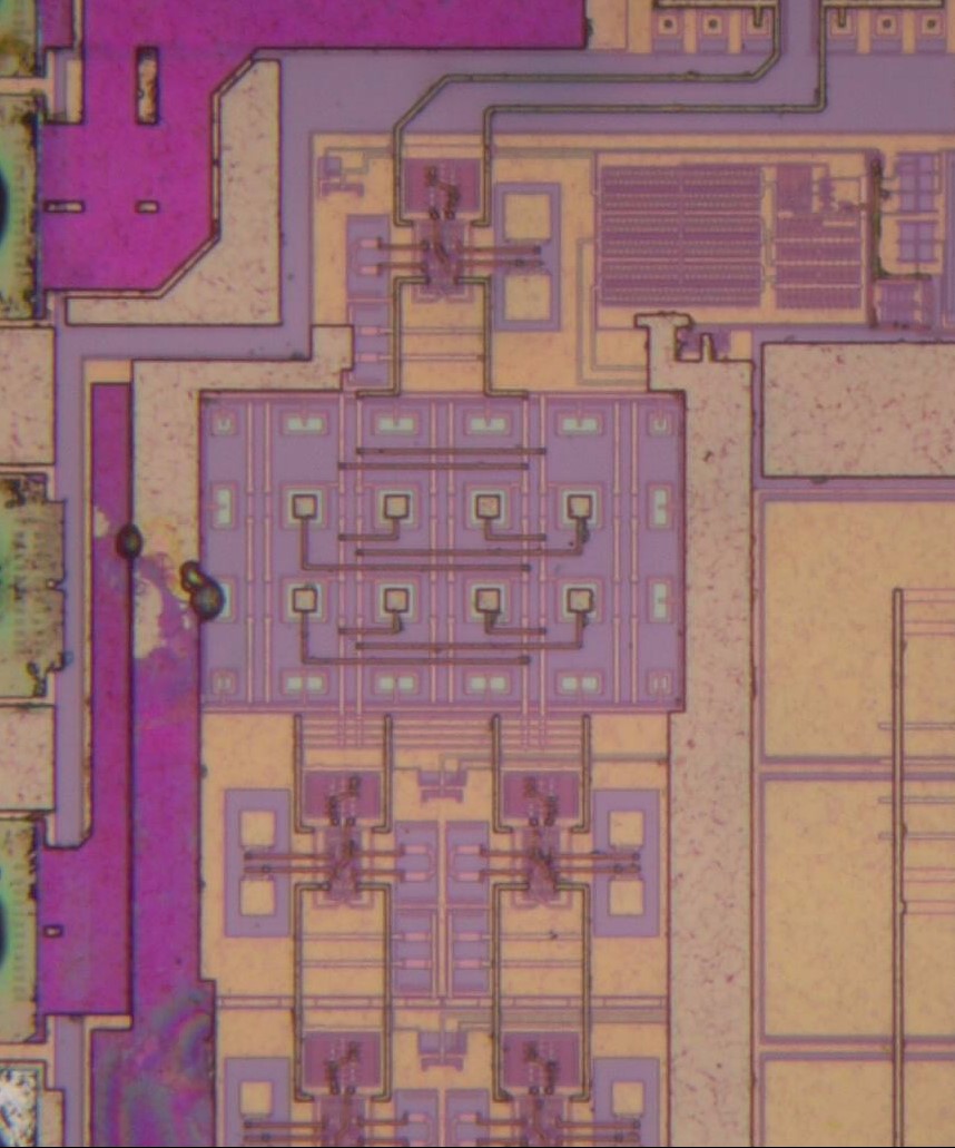
Here in the RF signal path we see what looks like a set of bipolar transistors (small squares). All circuits are nice and symmetrical, and take up a lot of space. The actual transistors are quite small, but the wiring, capacitors and clearance between the various parts takes up a lot of space.
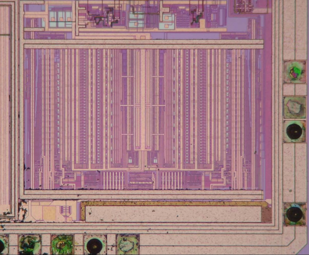
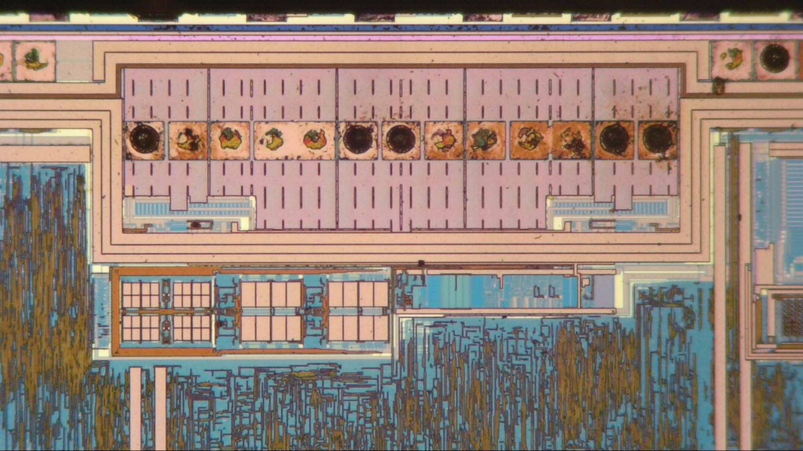
At the bottom right of the chip we find this enormous symmetrical structure. I’m really not sure what this is; it doesn’t look like any sensible circuit with its long vertical wires all over the place. Weird!
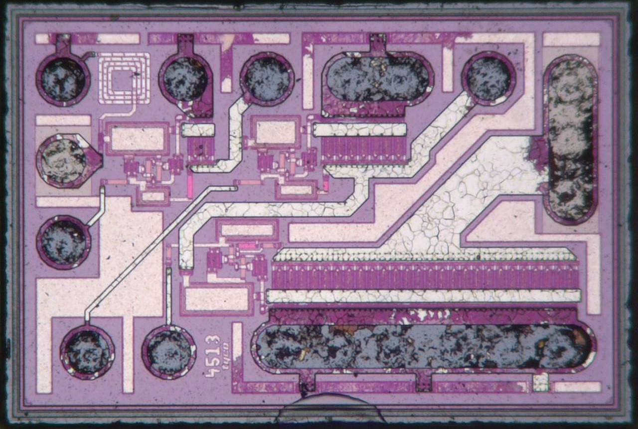
Finally, let’s look at the smaller chip in the phone’s RF section. On the package it’s labelled just “624 1914 29”, but inside we find a logo showing it’s made by Tyco and the numbers “4513”. However, searching any of these numbers gives no information about the actual part number or its exact function. Given the location on the PCB, and following the application schematic from the LMX4168 datasheet, this must be an RF Power Amplifier (PA). We see a big transistor on the right, between two large racetrack-shaped pads. It’s driven by a somewhat smaller transistor, just below the larger bond pad at the top, which is again driven by a still smaller transistor to its left. The three stages are AC-coupled through (rectangular) capacitors; each stage has a separate gate bias pin.
The top-left corner contains a single inductor, likely used for input matching. Specialized RF chips like this one are often produced in an IC process that’s suitable for high-frequency amplification but not so much for digital or low-frequency analog circuits. That’s why this is a separate chip, rather than being integrated into one of the other chips.