The 486DX series were the complete, full-performance versions of the 486 processor line. Unlike the low-cost 486SX, the DX versions contain an FPU, which significantly speeds up floating-point calculations compared to the earlier 386. In 1992 Intel delivered another huge leap in performance by simply doubling the clock frequency of the 486 core from 33 to 66 MHz. Motherboards at the time could not cope with such high speeds, so the bus clock remained at 33 MHz. Although 40 and 50 MHz speeds were also available, the 66 Mhz version was by far the most common and remained the processor of choice for most high-performance 486 computers until Pentium systems became mainstream around 1995.
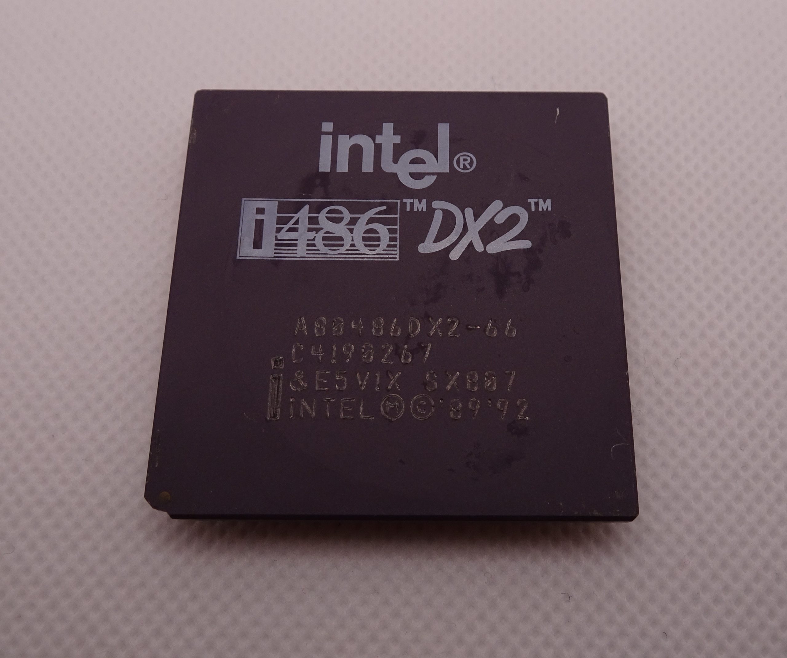
This is the ceramic PGA package that houses the DX2. This is an SX807 revision, which includes power saving features.
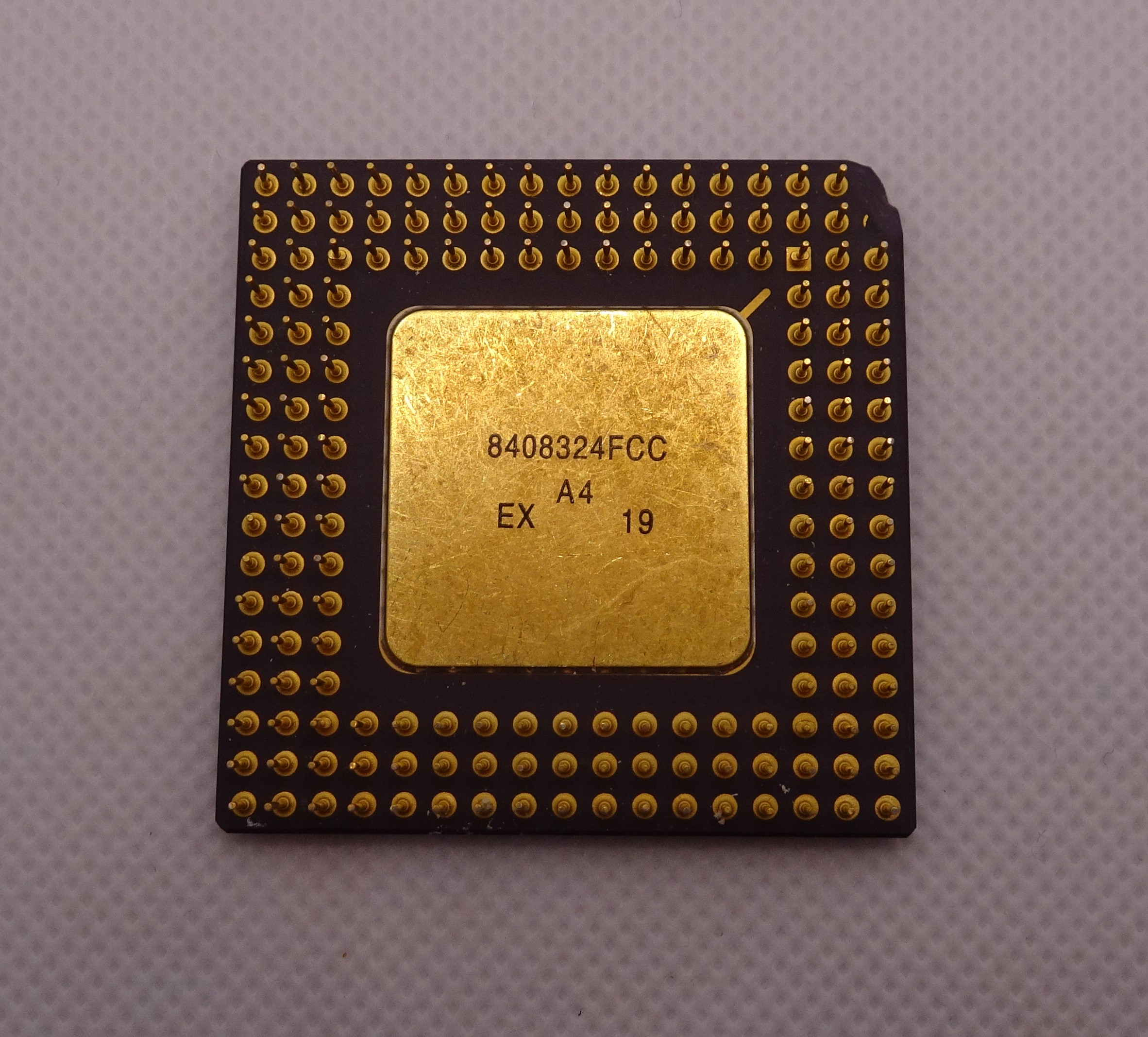
Here we see the pins at the bottom. There used to be 168 of them, but somehow this one lost two at some point in its life. I don’t know how, since these packages are nearly indestructible, although it is rather easy to bend the pins.
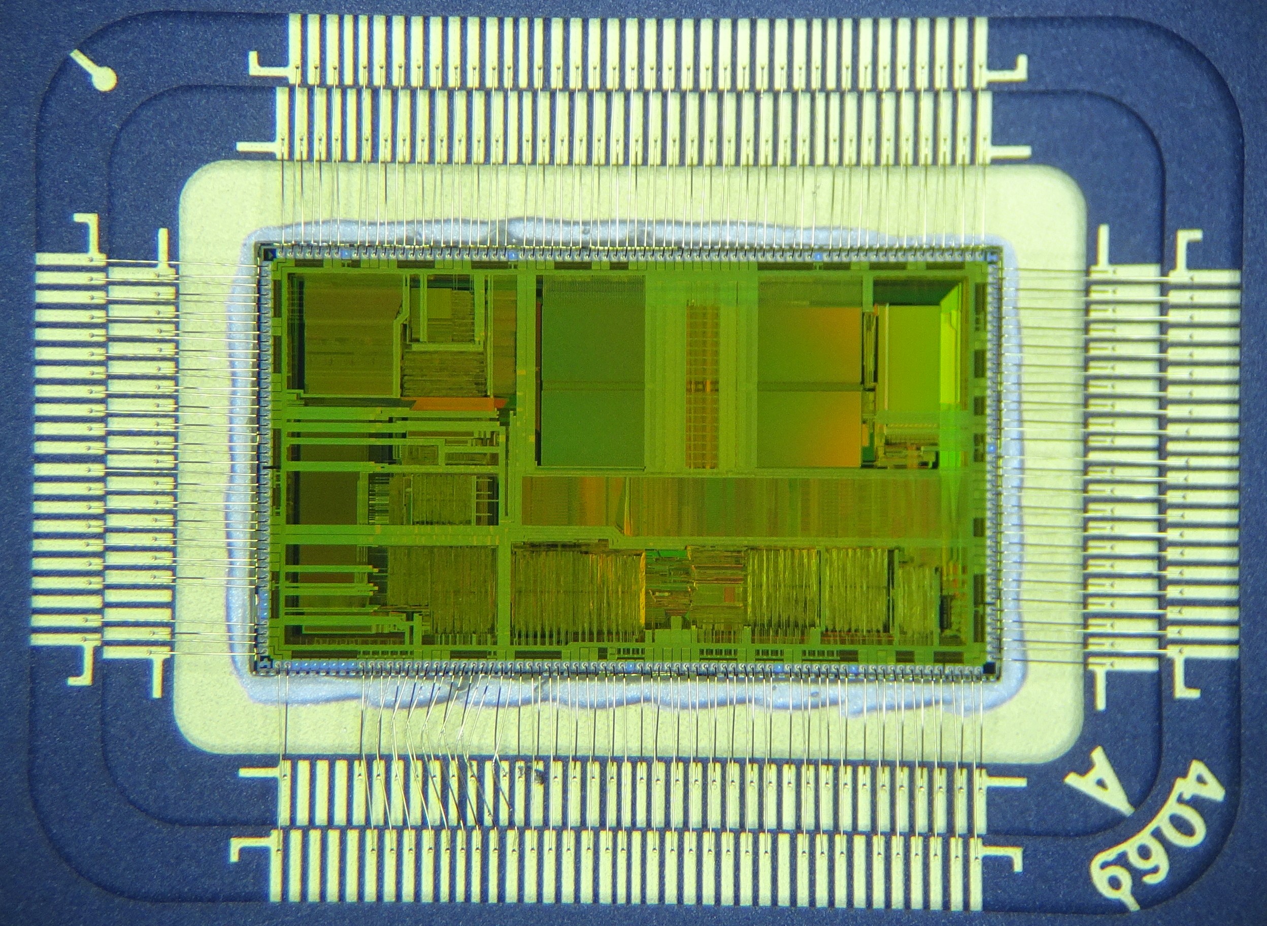
After popping off the lid, we’re greeted by a rectangular die, bonded to the package with shiny gold bond wires.
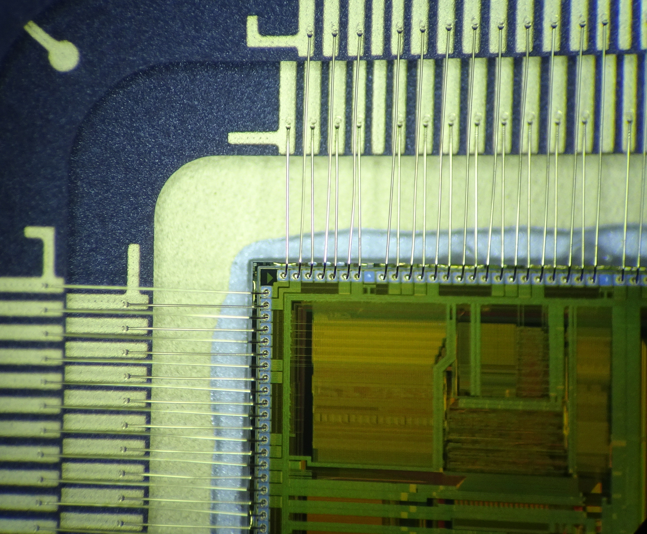
Interestingly, a few bond wires are skipped on the package as well as on the die, while the pads appear to have been probed. They’re apparently used for production testing.
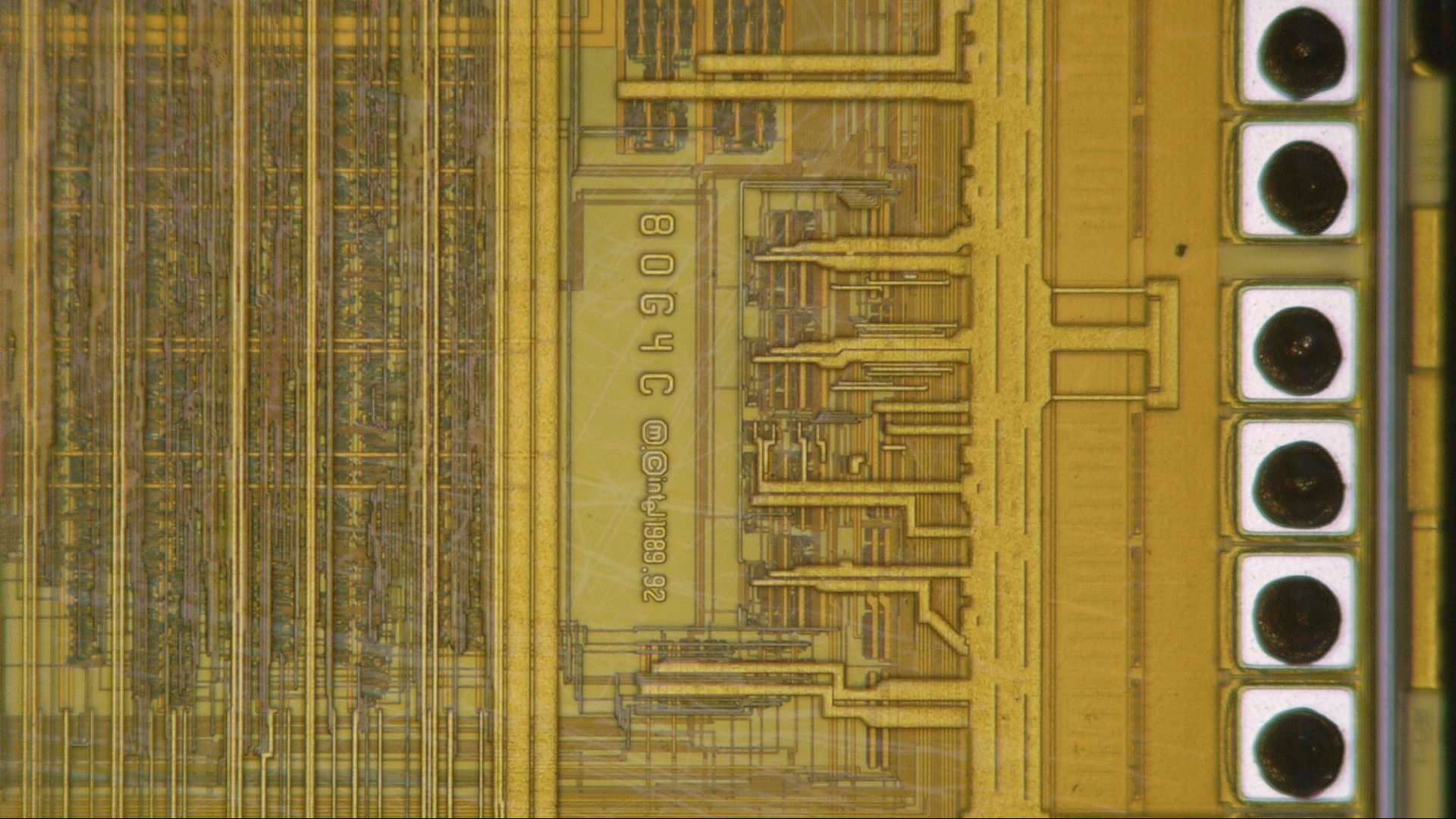
Zooming in on the copyright date, it appears that Intel calls it 80G4C internally, and this fact is indeed mentioned on a datasheet I found online.
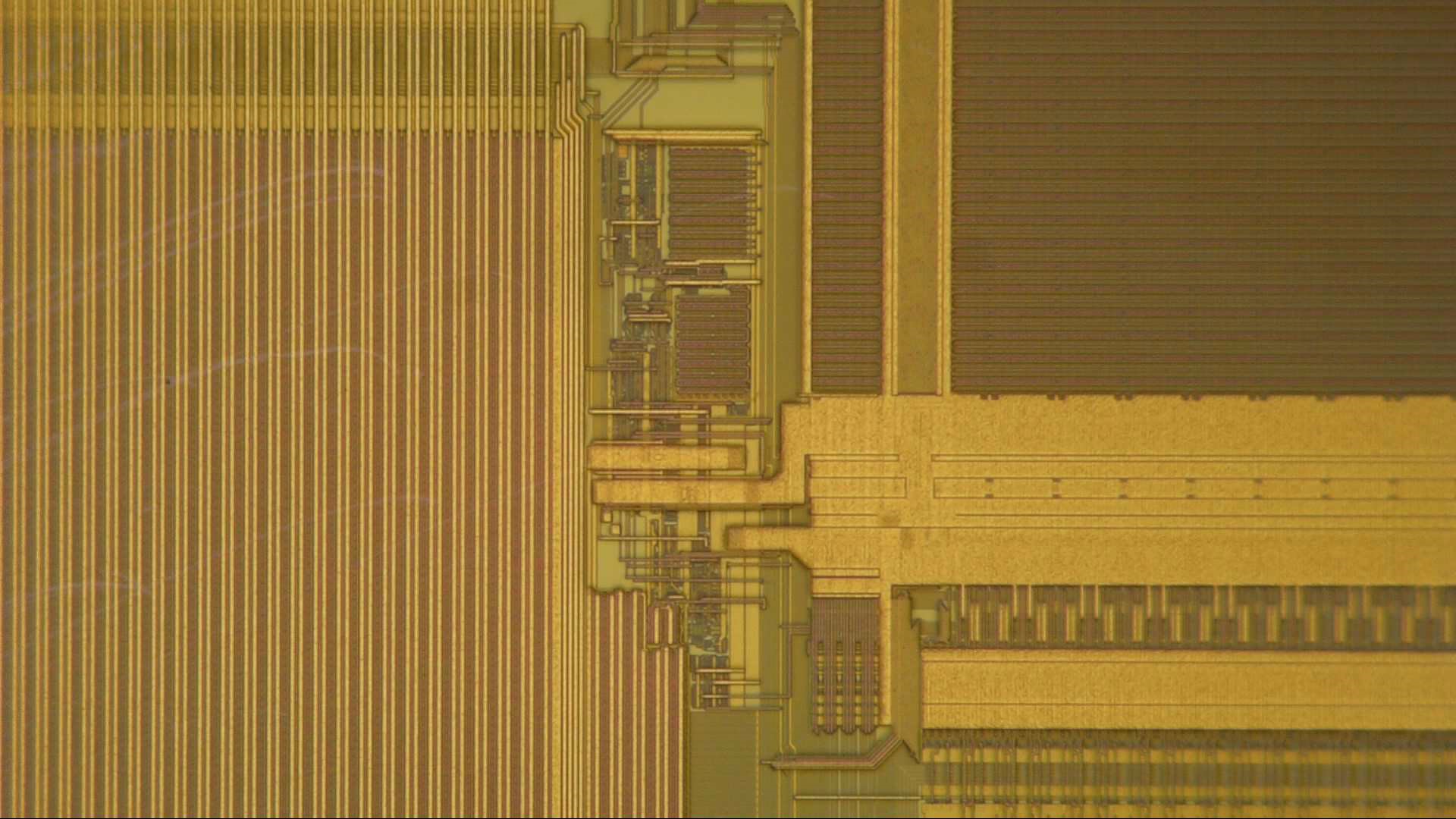
The die contains many buses, memory areas (among which 8 kB of cache) and logic.
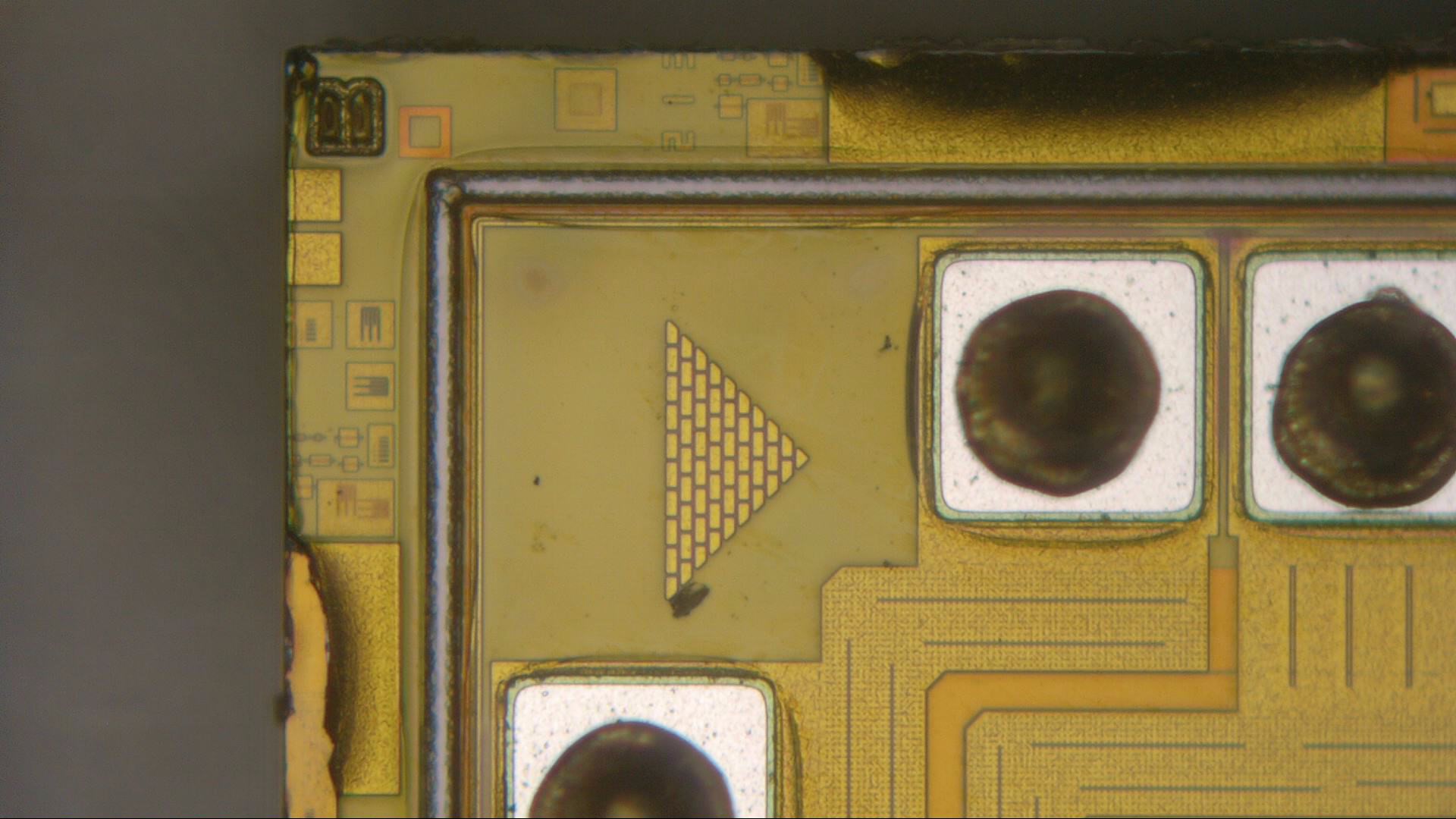
At the top-left corner there’s a little piece of chip art in the form of an Egyptian pyramid. Right along the edge we find the remains of several test structures which are used to characterize the performance of the production process. These structures are destroyed when the wafer is diced into individual chips.
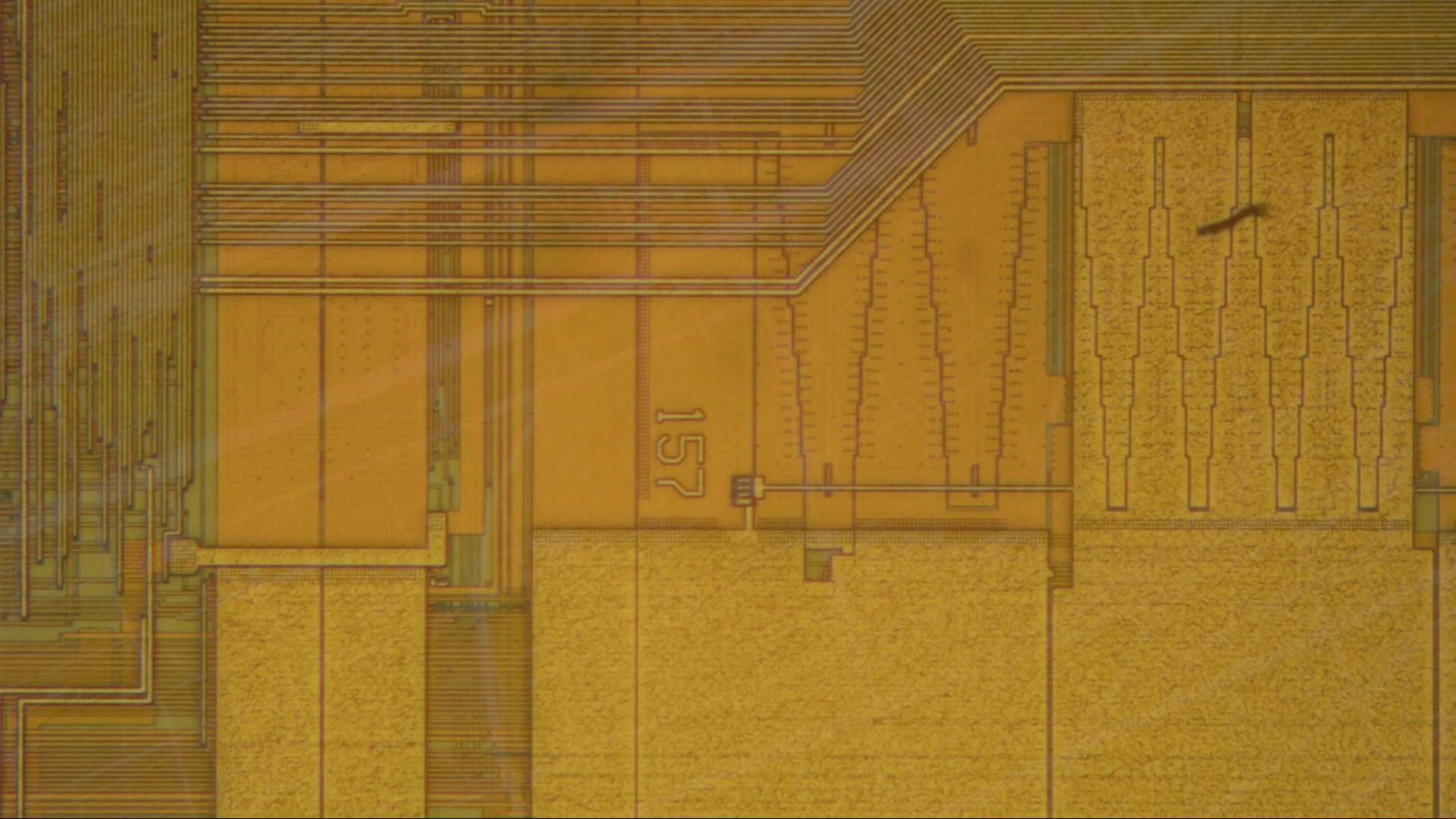
Near the lower edge we find a couple of large driver transistors, recognizable by the zig-zag shaped metal. These are likely used for power distribution along the chip. We also find the number “157”, but it’s not clear what that means.
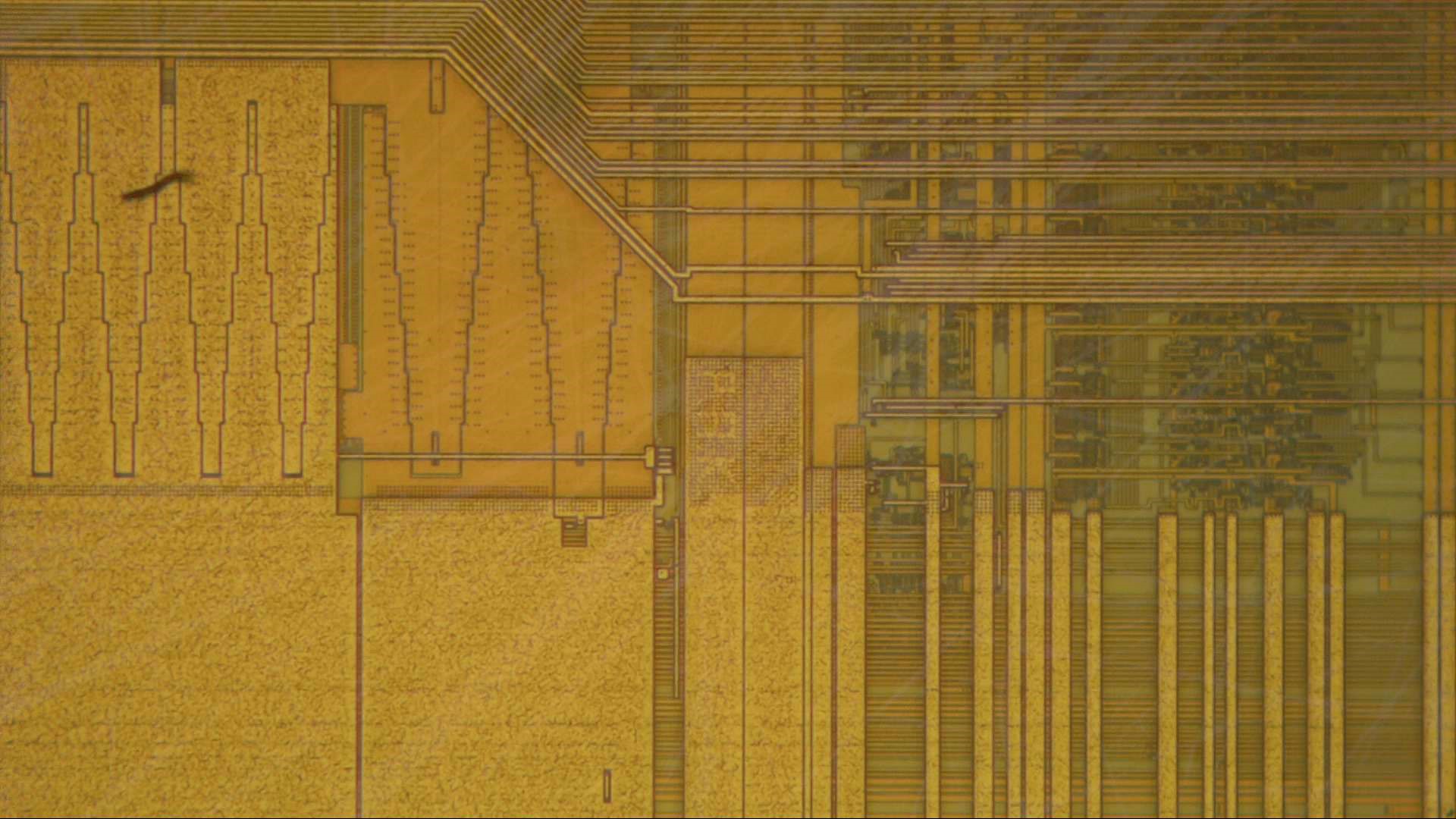
At the other side of the power transistors we find the letters “PAK” written in a group of vias. It’s the only set of letters I could find, and I’m not sure who or what it refers to. The 486’s lead architect was Pat Gelsinger, who was recently (early 2021) announced to become the next CEO of Intel, but these letters don’t completely match his name.
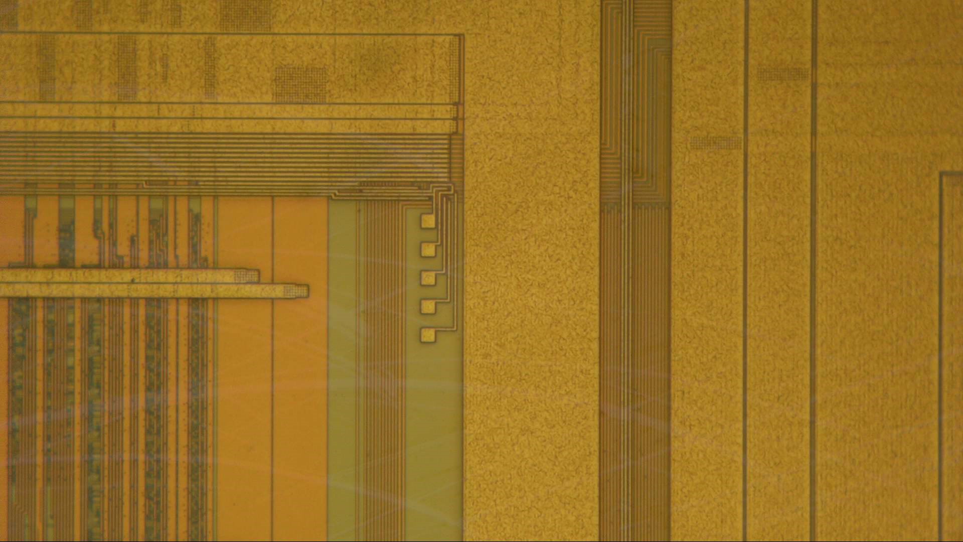
Somewhere deep inside the chip are these five little squares. They could be test pads, used for debugging. They are way too small to be used for production tests: we’re looking at maybe 10×10 microns, while normal probe pads are usually 100×100 microns (like normal bond pads). Also, the passivation is not removed at this place, so the probe pads are not normally accessible. What generally happens is that a few test chips are specially processed to not have the final passivation layer (which normally protects the chip from dust and moisture), and a special probe station with very sharp needles is then used to probe these little pads and access internal signals.