The LIS3DH is an accelerometer, designed and manufactured by STMicroelectronics. Like most accelerometers today it is a MEMS device (Micro-Electro-Mechanical Systems), which means the sensing function is made from silicon and integrated into an IC process. Special etching techniques are used to create tiny moving parts that can bend in certain directions, along with sensors that can detect that movement.
MEMS accelerometers are used in many electronic devices: your phone that detects whether you’re holding it horizontally or vertically, your games console that can sense which way you’re moving the controller, or your car that can detect the speed and direction in which you’ve just crashed so it can properly deploy the airbag.
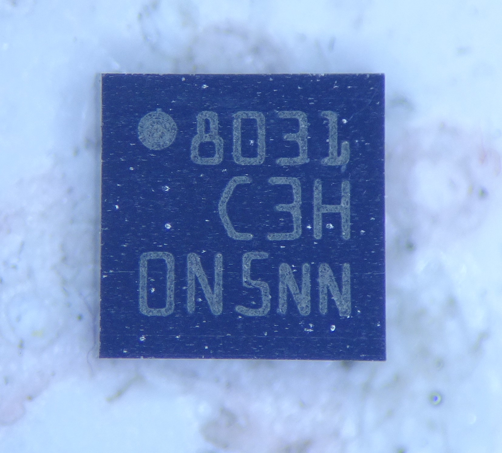
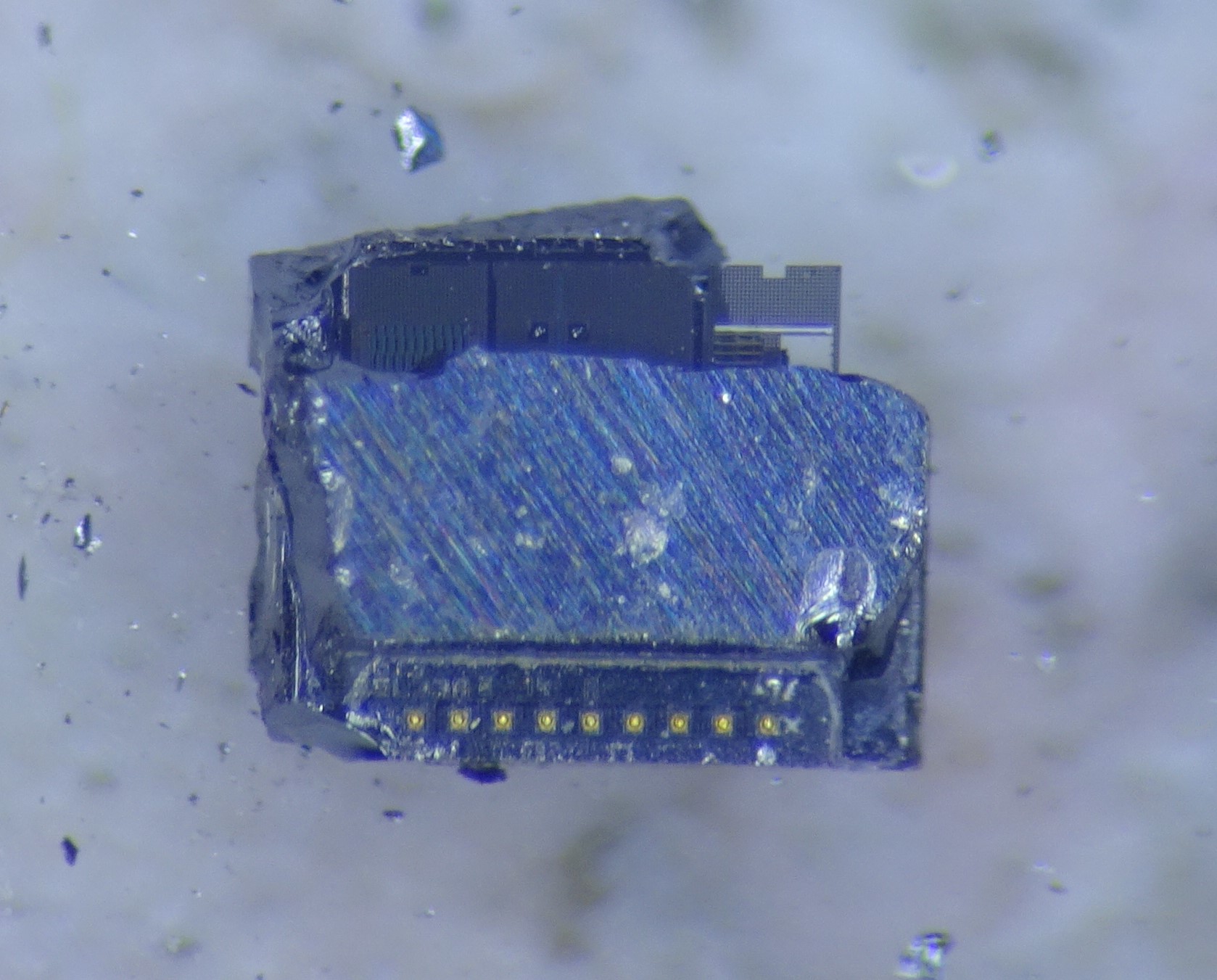
The LIS3DH is housed in a little LGA package that measures just 3 x 3 mm2. Oddly there’s no ST logo or marking on the package. The “ON5nn” production code could actually trick you into thinking this is an ONSemi part.
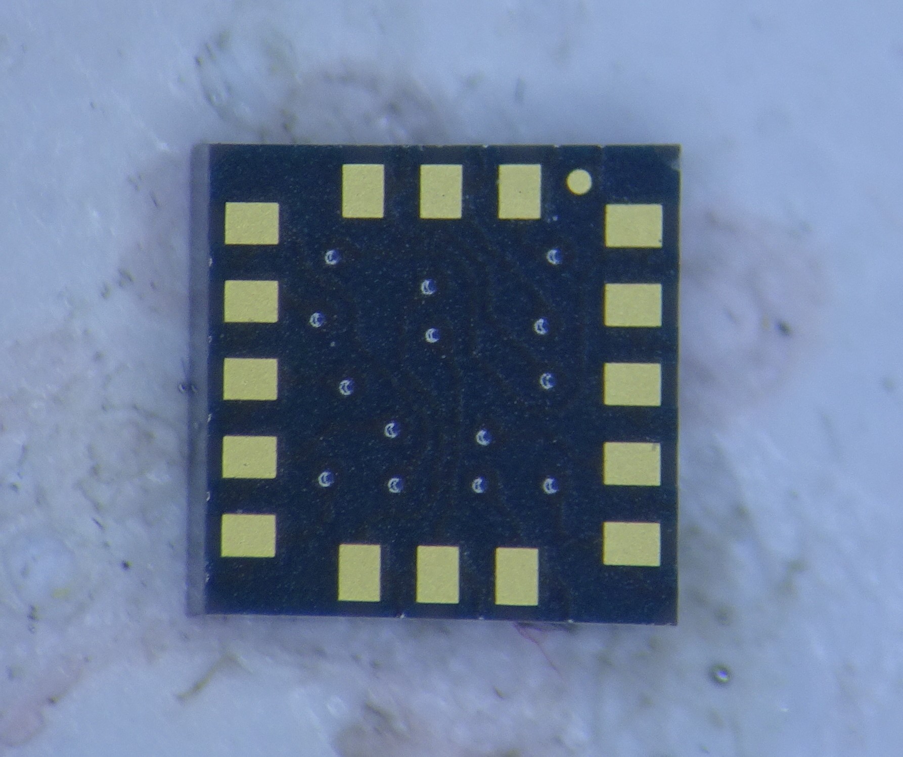
On the other side we find the mounting pads. We also find traces and vias on the bottom, indicating this isn’t a simple wire-bond package but a somewhat more complicated package that needs signal routing inside. The bottom layer is basically a very small PCB, on top of which the actual IC is wire-bonded. That assembly is then covered in epoxy, which forms the body of the package.
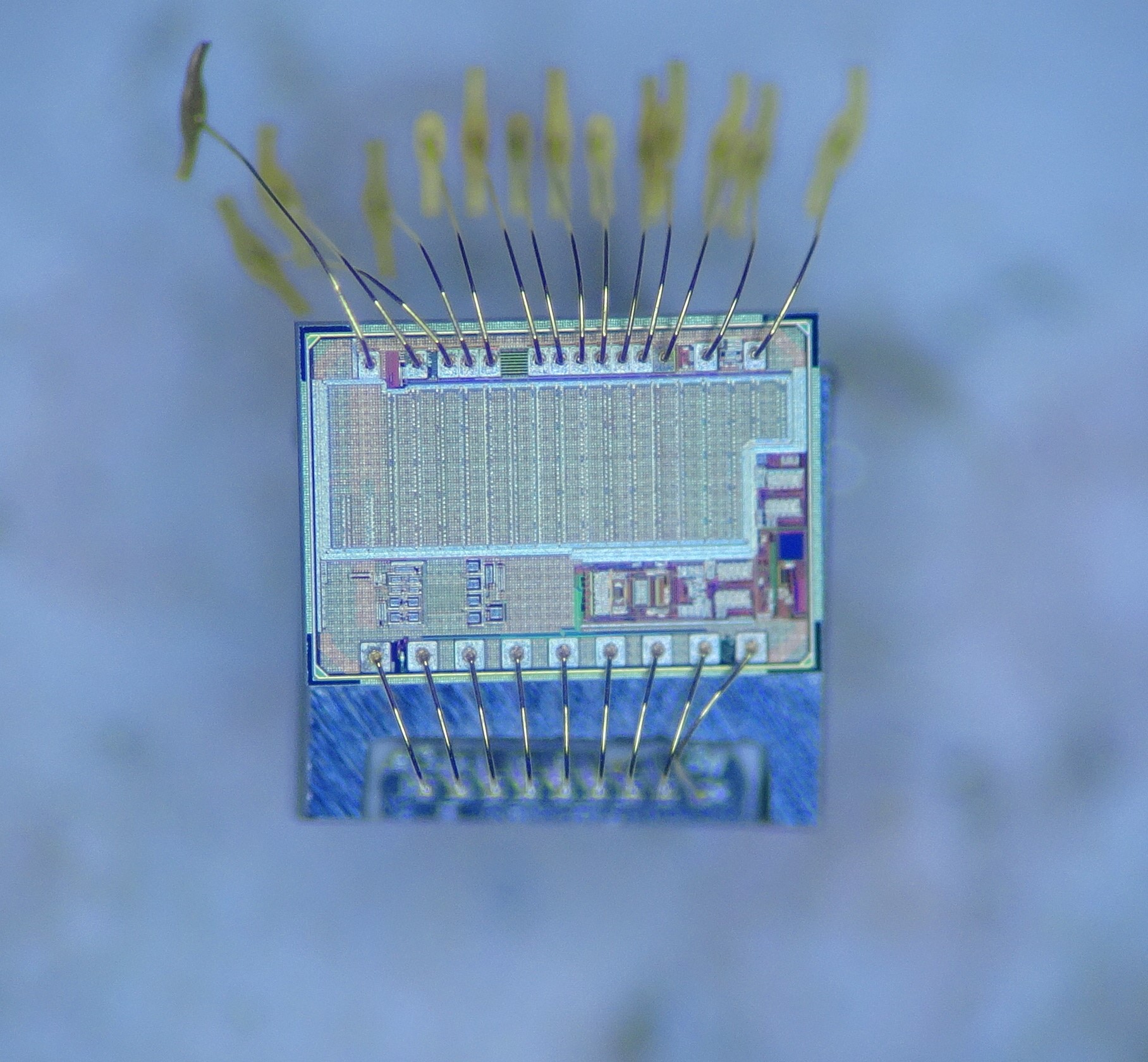
Once inside we find this interesting stack. At the top there’s a signal readout IC, connected to the package through the top row of bond wires. Its job is to read out the sensor and convert its analog signals to digital. Below this chip is the actual sensor chip, connected to the readout IC though a second row of bond wires.
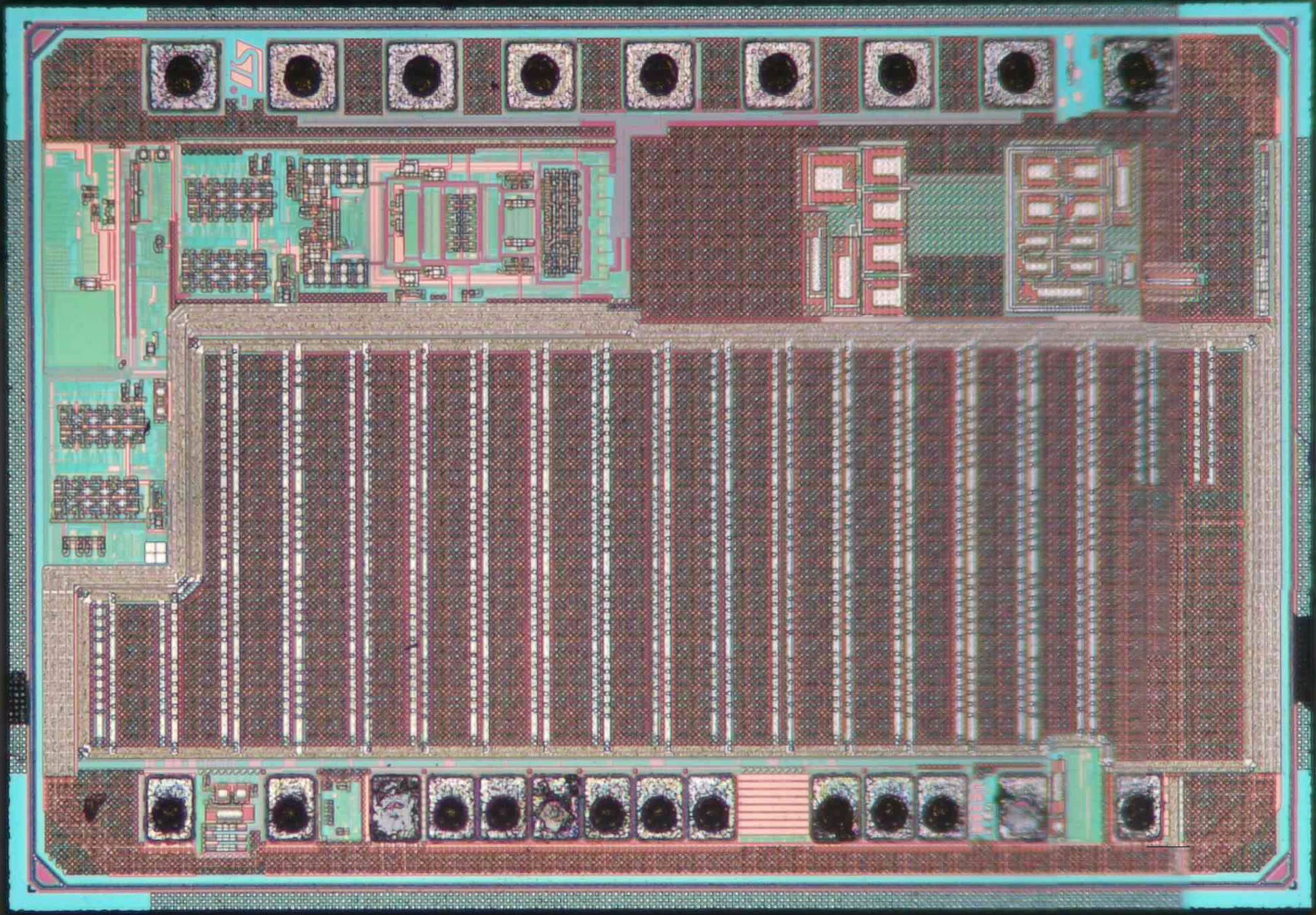
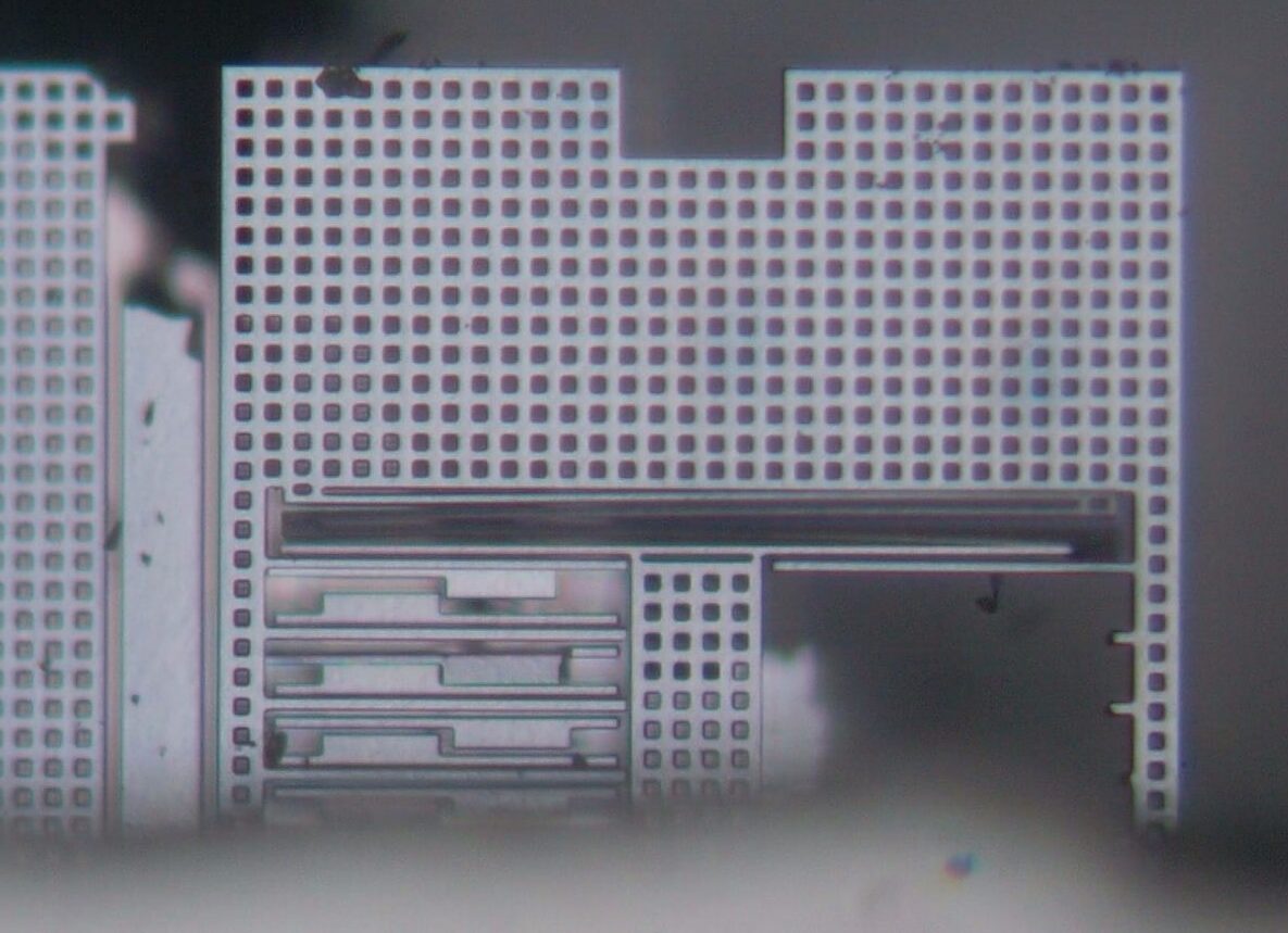
The readout chip is made in a reasonably modern process, and its layout is very typical of a mixed-signal chip: a digital part (about the bottom two-thirds) plus some analog circuits (at the top and top-left). The sensor chip connects at the top, near the analog circuits, while the digital interface connects to the bottom row of bond pads.
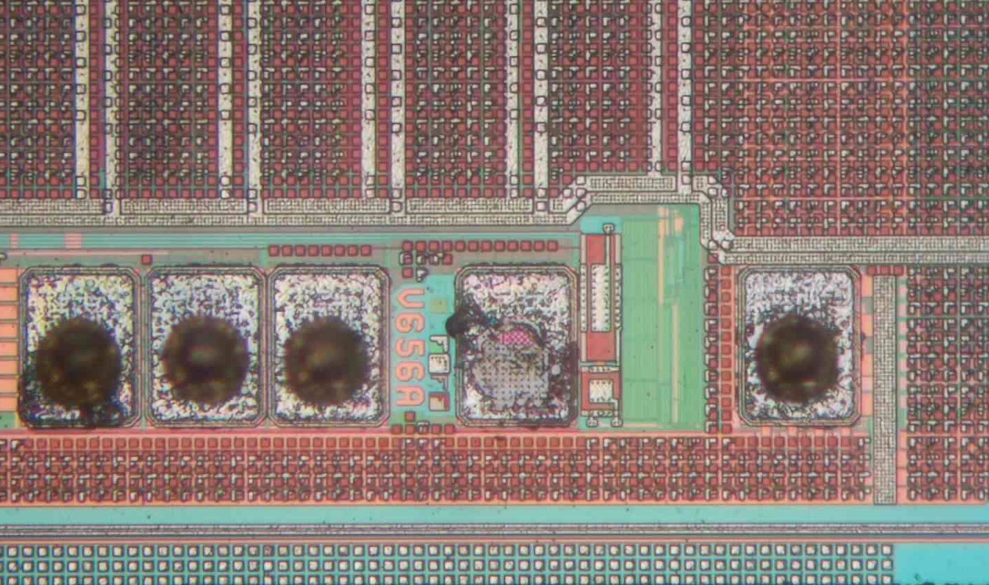
Apparently this chip’s internal part number is V656A. Most of the internal circuits are obscured by dummies: little squares or L-shapes that ensure a consistent metal coverage on each layer.
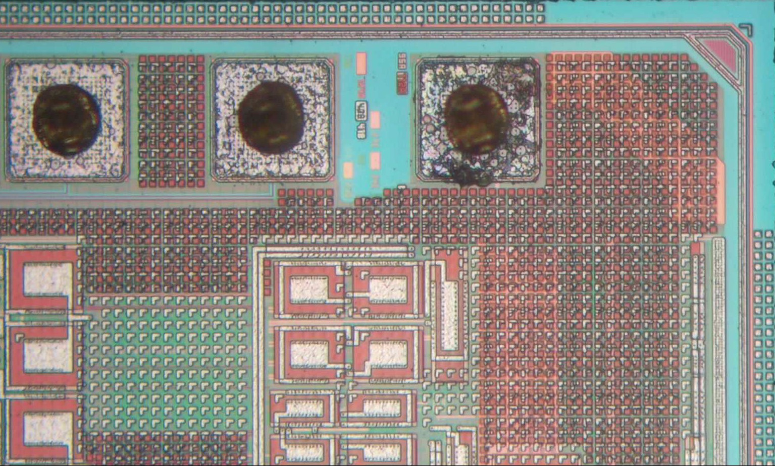
At the top-right corner we find the layer markers and some shapes that look like capacitors.
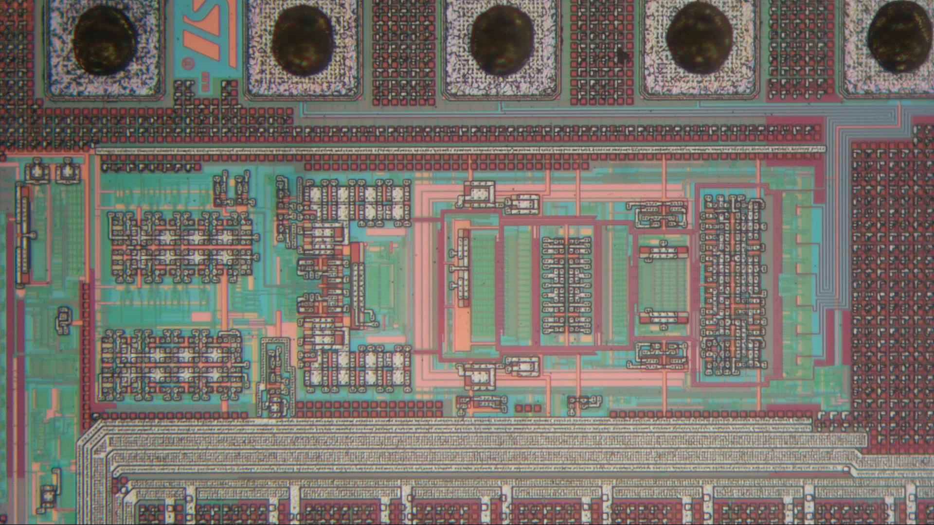
Here are the analog circuits that interface directly with the MEMS chip (note the bundle of wires going to the bond pads at the top row). This probably consists of an amplifier and an analog-to-digital converter. At the top we find the ST logo and a 2010 copyright date.

The second chip inside the package is this one, the MEMS chip that contains the actual accelerometer. It’s completely sealed; the datasheet mentions that the MEMS die is covered with a special “cap” to ensure the plastic from the package doesn’t clog up the moving parts. As it turns out, this cap is a second piece of silicon that’s placed on top of the MEMS chip, with a cut-out to expose the bond wires.
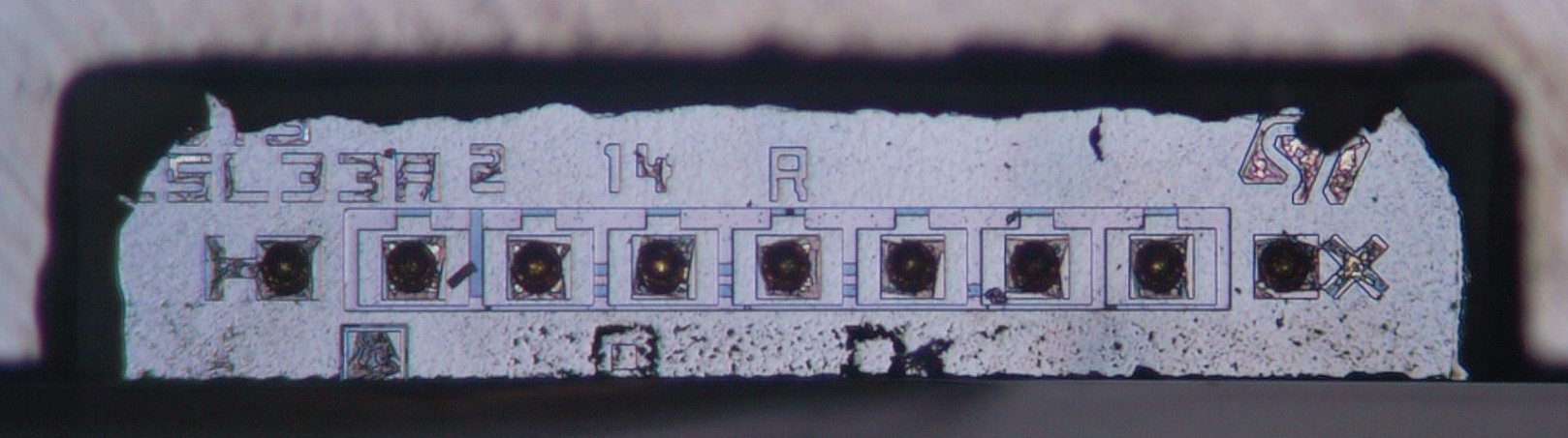
This MEMS die has an internal part number ending in “SL33A”. It’s clearly made in a much simpler process; this makes sense, because it should really be optimized for creating sensors, which means that just one simple metal layer might be enough.
Unfortunately, the top layer is very well bonded to the bottom chip and I couldn’t open up the whole thing without severely damaging both halves. The whole thing is only about 1.5 mm wide and 1.8 mm long, making it very tricky to perform any kind of mechanical work on it. But luckily, enough of the chip survives to show us how the MEMS sensor works.

Here is the part that senses acceleration in the horizontal direction. The main mass (with all the square holes) is hanging from a few points and can swing to the left and right. The vertical beams then sense that movement: the capacitance between the beams and the frame is measured, which tells you the amount of acceleration. Those beams are attached to the base of the chip and do not move.

In the middle is a section that measures acceleration in the Z direction (up and down in the plane of the chip). The whole frame can flex up and down, again changing the capacitance to the stationary part of the chip.
Finally, this section measures acceleration in the vertical direction. You can see the beams in the left half of the picture; those on the right have broken off with the base of the chip, leaving a hole in the frame. Note how this whole section is now actually floating in air! It’s an extremely thin piece of silicon but still strong enough to support its own weight.
Overall I’m surprised by how much technology is inside this chip. I was expecting just a single chip with some MEMS structures sitting next to the signal processing, but instead there’s two separate chips, one of which has a rather complicated setup with a second hollowed-out chip sitting on top. It’s almost unbelievable that all this can be bought for about €1!