Today we’ll look at a couple more versions of the 555 timer. Like the 741, this chip has been produced by many different manufacturers in the nearly five decades since its introduction by Signetics in 1972.
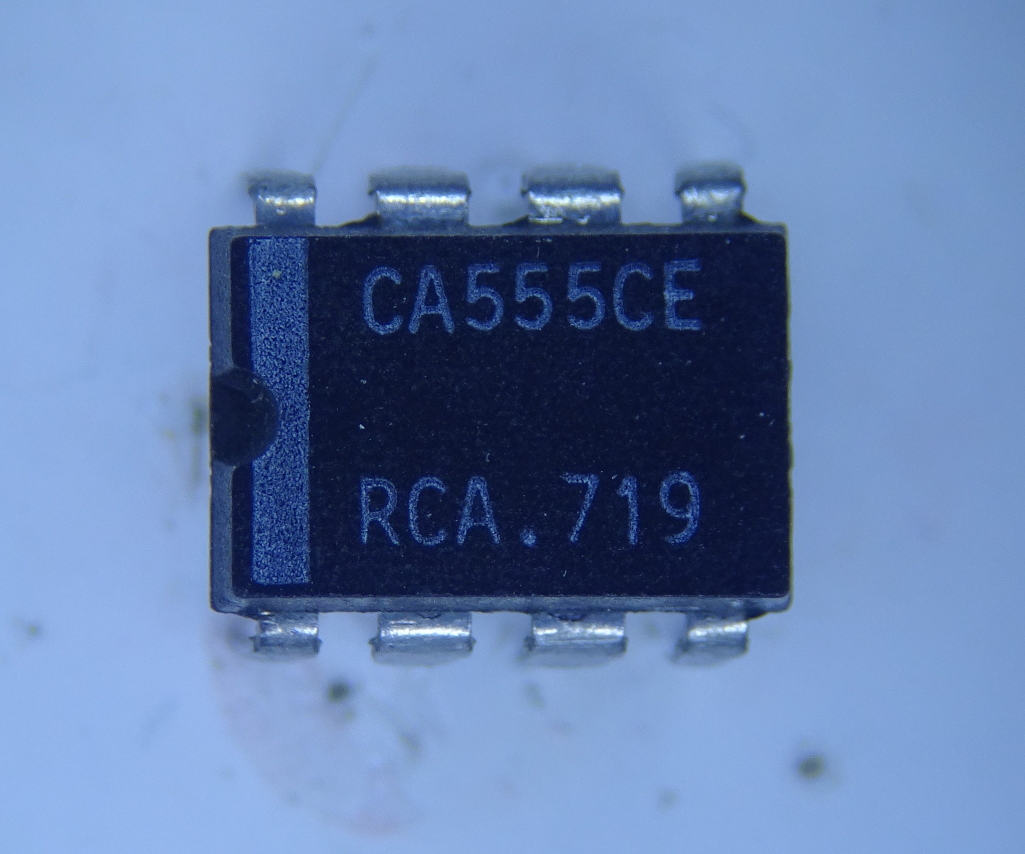
First up is RCA’s CA555. Packaged in an 8-pin DIP (which is what the “E” in “CA555CE” stands for), this is a “C” spec which can work at up to 16 V, unlike the CA555E that is spec’ed up to 18 V. I’m not sure what the actual difference between these two would be; I guess the chips were sorted after production, with parts that marginally failed some spec at 18 V being demoted to “C” versions.
The date code is not entirely clear; it cannot be from 1971 since the 555 was not yet introduced at that time. The CA555 is featured in a 1975 catalogue, so it was introduced shortly after the Signetics original, but the package looks too new to be from that era. My guess is that it’s from the late 1980s, sometime before 1988 when RCA’s semiconductor division was sold to Harris.
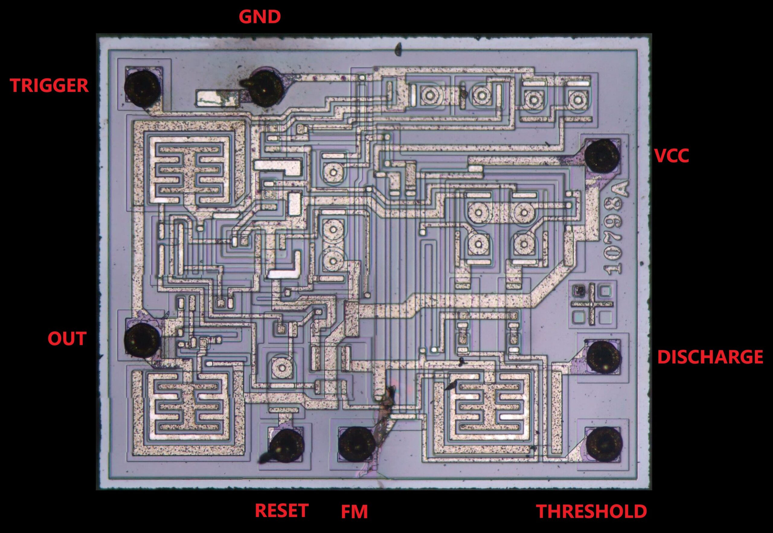
Inside we find a design typical for the 1970s and ’80s, with round PNP emitters and lots of empty space. The design is the same as Hans Camenzind’s original schematic. Note how the GND pin has a round bond pad, with a large rectangular substrate contact to its left.
On the right side we find internal reference code “10798”, revision code “A” and an alignment target consisting of a metal “+” shape with squares of various layers in its four corners.
Next up is the Harris CA555T. This one has a 1994 date code and was apparently assembled in India.

The product code starting with “CA” is actually a clue to this specific chip’s provenance: as I mentioned already, Harris acquired RCA’s semiconductor division in 1988, so it makes a lot of sense to see RCA’s old product code on a Harris chip.

Inside it’s completely identical to RCA’s chip above; not even the mask revision has been changed. Harris clearly left RCA’s design untouched for at least six years.
Five years after this chip was made, in 1999, Harris spun off their semiconductor operations to form Intersil, recycling the name from another manufacturer they acquired together with RCA in 1988. However, it looks like the new Intersil discontinued the CA555, offering only the ICM7555, a CMOS version.
Another 555 timer in a classic metal can package is the TDB0555 by Siemens:
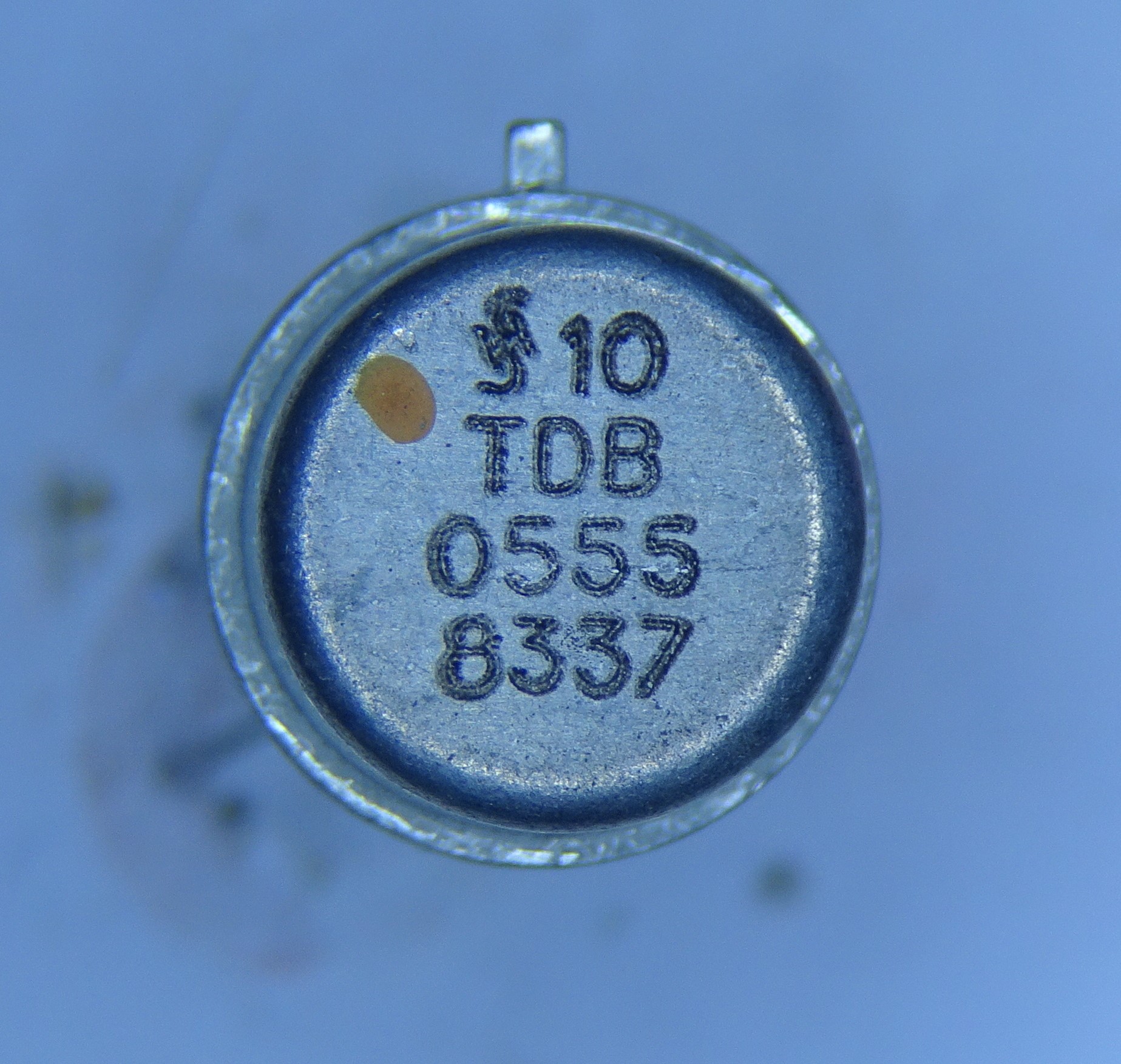
The brand name is identified by the old “SH” logo, representing Siemens & Halske, one of several Siemens companies that merged in 1966 to become today’s engineering conglomerate. The SH logo was largely out of use in the wider Siemens group by the 1970s, but was apparently kept for the semiconductor business (perhaps because it might stand for “Siemens Halbleiter”?). This chip dates to 1983; Siemens spun off their chips and transistors to become Infineon in 1999, but discontinued the 555 somewhere between these two dates since it was never produced under the Infineon brand.
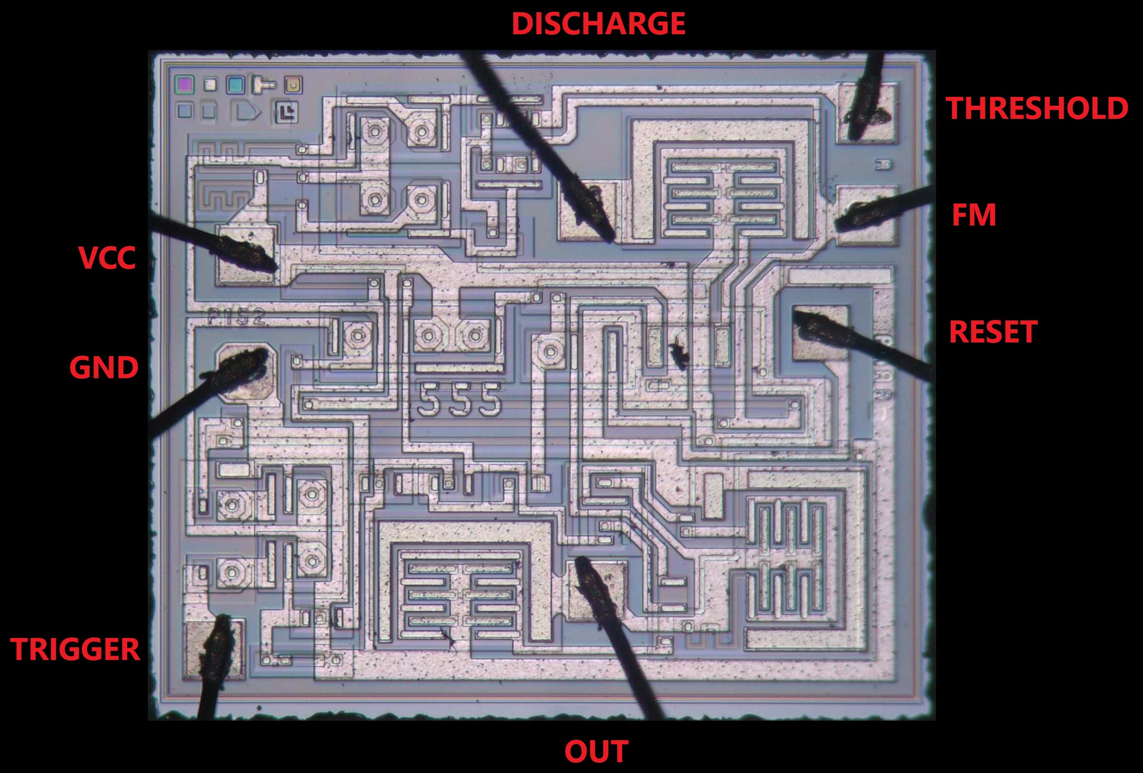
Once we look inside, the picture becomes a bit confusing: this is exactly the same chip as Thomson’s TBD0555 that we saw last time. Now Siemens, which became Infineon, and Thomson, which became ST, are still rivals to this day, so it’s somewhat surprising to see them developing a single chip together. I can’t figure out how this might have worked: although Siemens and Thomson did collaborate at one point, in a consortium with Philips named JESSI (Joint European Submicron Silicon Initiative), this only began in 1989 and was focused on developing state-of-the-art chips, not generic old stuff like the 555.
The only reasonable explanation I can think of is that either of the two companies developed this chip, with the other licensing its design and selling it under their own name, in order to plug a gap in their portfolio without having to develop it from scratch. Then again, this is such a simple chip that any manufacturer with a bipolar process should be able to develop it within a few weeks (as everyone did in the early ’70s).
Next we’ll look at the chip that is actually the real, original NE555: the one made by Signetics.
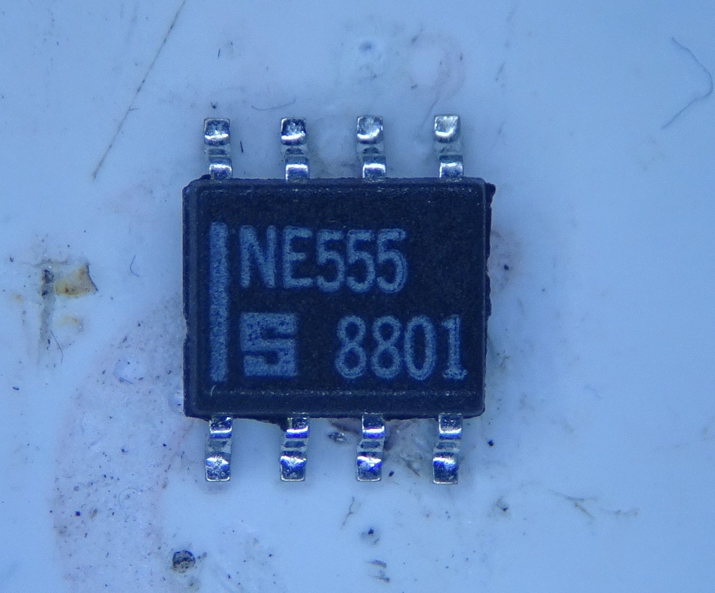
Signetics, recognizable by its thick square capital “S” logo, originally introduced the NE555 in 1972, after Hans Camenzind developed it under contract. The chip seen here is an SO-8 version with a 1988 date code.
Inside it looks just as you’d expect. The three power transistors are clearly recognizable. The three 5k resistors (R7, R8 and R9) are laid out vertically in the middle of the die. There is a part number “4190A” at the top, but no manufacturer logo or “555” text anywhere.
Along the bottom edge we find mask identifiers: 1A, 2A, 3A, 4A and 5A. Apparently all five are in their first, or “A” revision. The bottom left has an alignment marker, and there’s a rather odd thing just to the right of the VCC pad: a rectangular shape with two unequal squares at the top and bottom. This could be another test structure, maybe to be probed on those two squares as well as the VCC wire just below it.
Signetics was acquired by Philips in 1975, but continued as a separate brand for several years. Eventually the NE555 was also released under the Philips brand. Production came to an abrupt end on 12 December 2003, when a fire in Philips’s wafer fab in Caen (France) destroyed the production line. Philips released a list of products that had to be discontinued because of this fire, still available on NXP’s website, which includes all varieties of the NE555. It was a sad end to a 31-year production run.
However, the design lives on in all the clones made by other manufacturers. One of the big ones still making the original 555 today is STMicroelectronics:
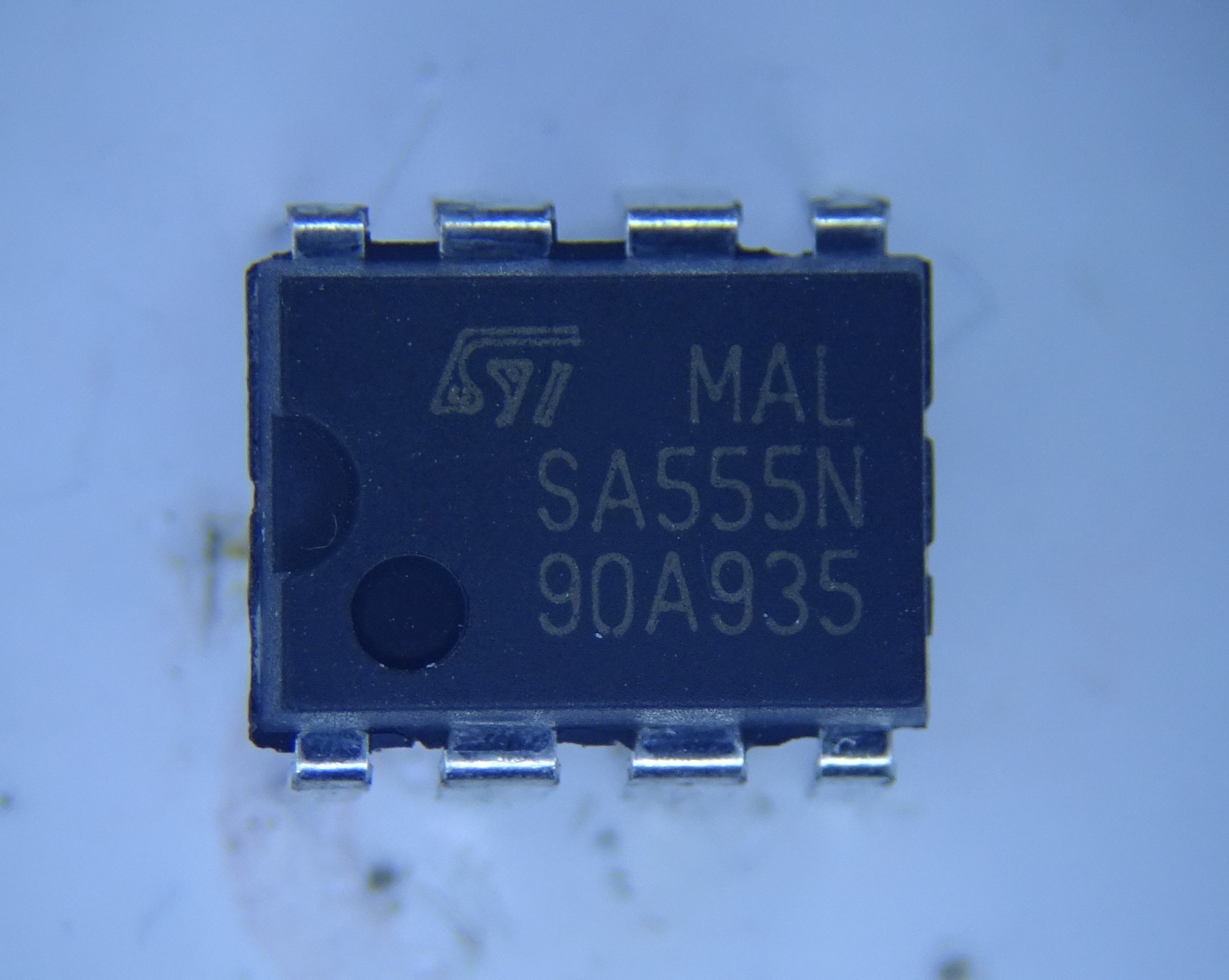
ST was formed from Italy’s SGS and France’s Thomson in 1987. This specific chip seems to be brand new, though I can’t decipher the date code.
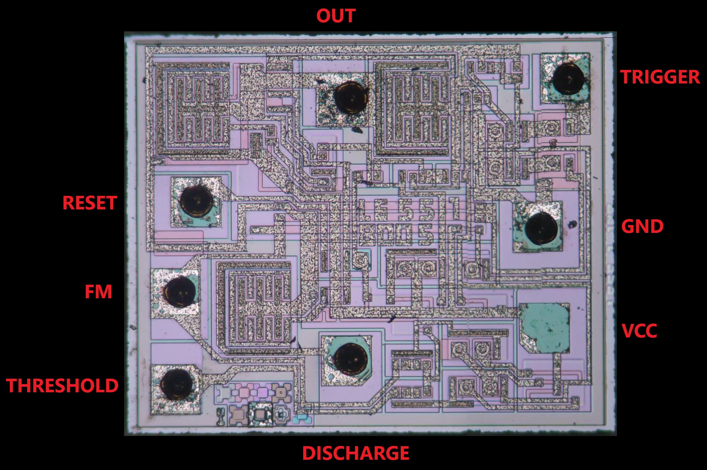
On the inside however, it looks like a rather old design, quite like the ones we saw above. There’s an identifier in the middle of the die, consisting of rather crude characters that spell out something like “L6551 8005”. Clearly those three 5’s belong together, but what the rest means is anyone’s guess.
The layout actually looks rather similar to the one we found in the Thomson chip last time and the Siemens part today. If you rotate either layout by 180 degrees you’ll see that nearly all components are located in the same place on both chips. This strongly suggests that the original design was by Thomson, not Siemens, since ST is the successor to Thomson.
The schematic is a hybrid between Camenzind’s original and National’s derivative that we saw last time: it has an NPN current mirror loading the Trigger comparator (immediately to the left of the Trigger pin), but also resistors R1, R2 and R3 at the Threshold comparator (bottom right).
The various wells and diffusions are clearly visible as different shades of pink, purple and blue. At the bottom-left there’s a series of alignment markers showing each of the layers in sequence. The metal layer has a rather coarse surface for some reason.
Finally, I found an NE555 from an unclear manufacturer:
The logo looks vaguely like TI’s, and is perhaps a poor attempt at copying it. Also, the exact part number “NE555P” is what TI calls its DIP packaged version.
Once inside we clearly see that this is not a TI part. In fact, we’ve seen this chip before: it’s the same one as inside HGsemi’s LM555. It looks like someone bought a batch of these and re-labelled them with TI’s part number and a similar-looking logo, to earn perhaps one cent on each one sold.