Today we’ll have a look at another chip that has absolutely earned its place in the history of electronics. Designed in 1986, the MAX232 represented a small revolution in IC design and put Maxim, then still an upstart, in the spotlight for the first time. Dave Bingham was the driving force behind the MAX232’s design, in a team led by Dave Fullagar (of UA741 fame).
The MAX232 became popular because it was very easy to use and it solved a common problem: many computer systems running on a single +5V supply used RS-232 standard serial interfaces, which required +/- 15 V signal levels. The MAX232 was a transmitter/receiver chip with a built-in charge pump that generated the required signal voltages directly from a +5 V supply, removing the need for two additional supply rails.
Clever marketing also made the MAX232 a huge success for Maxim. Putting a big “MAX” in front of its part number made it immediately clear who made the chip, unlike TI’s “SN” or National’s “LM”. The fact that the ‘232 became the most popular among Maxim’s MAX2xx series (which ran at least from MAX220 to MAX249 back in the day) could be either because that number matched its RS-232 functionality, or simply because it had the most commonly used combination of channels (two transmitters and two receivers).
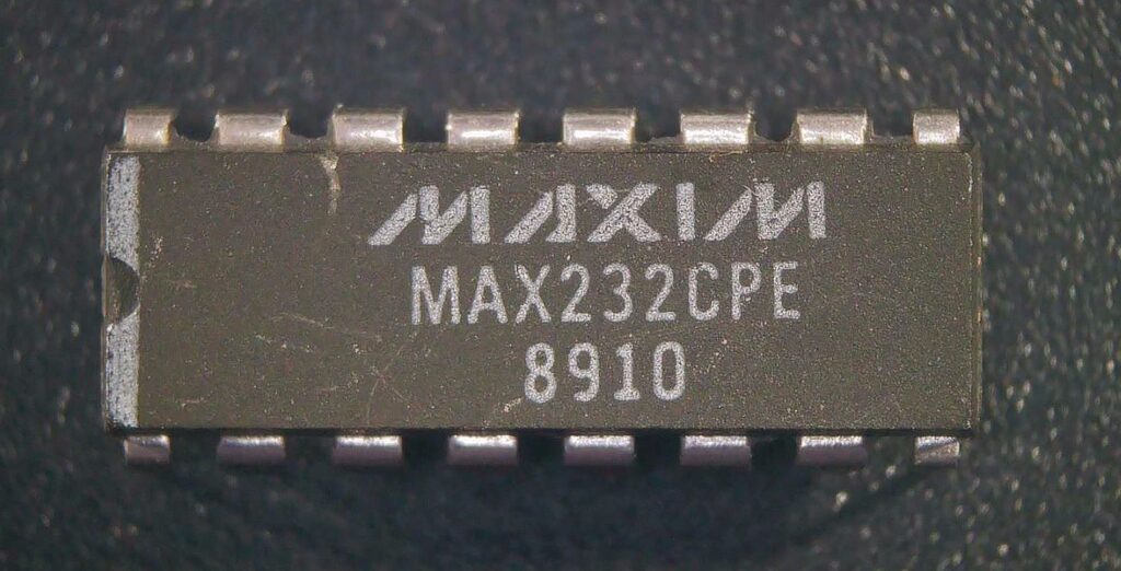
Maxim has since expanded its RS-232 transceiver range to include dozens of different models with varying numbers of channels, different supply voltage ranges (like the 3V MAX3232), power-down options (MAX242), and even integrated capacitors (MAX233) and isolation transformers (MAX252). But the classic MAX232 seems to remain its most popular model. I dug around in my parts bin and found this MAX232CPE from 1989. It’s housed in a 16-pin plastic DIP package.
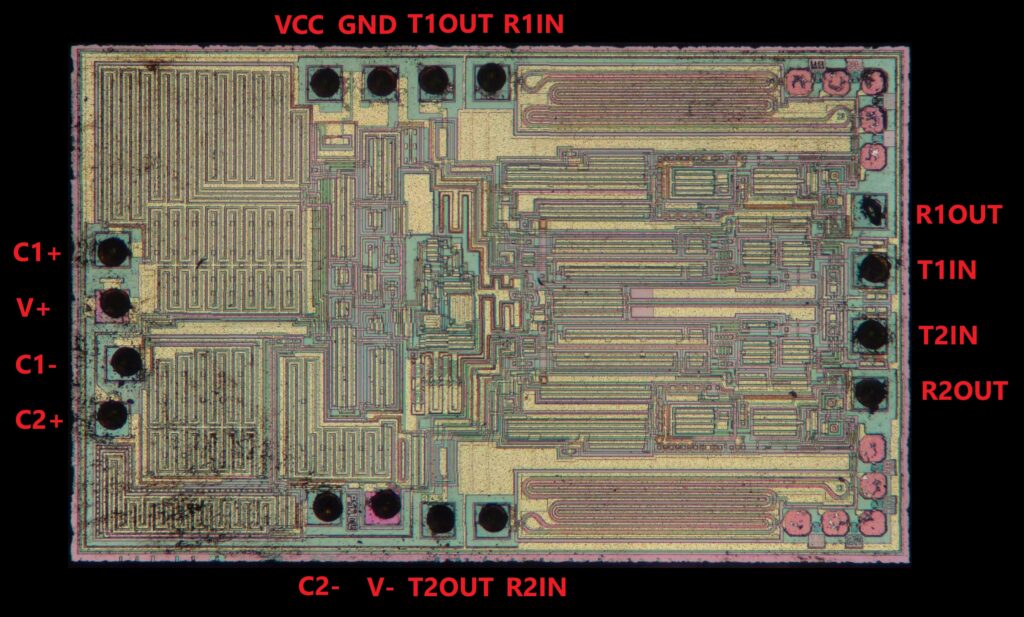
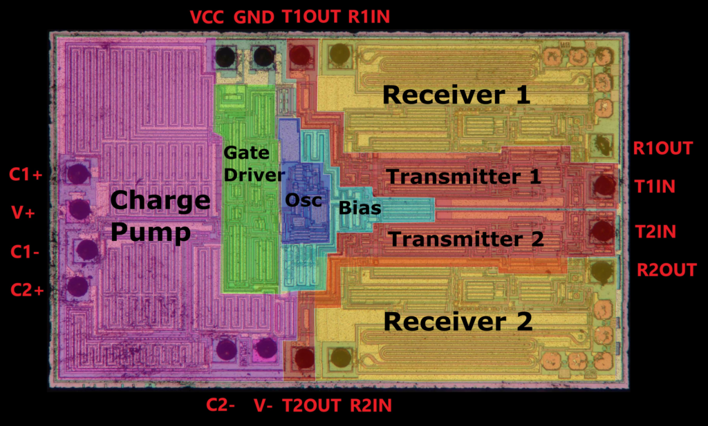
If we open it up, we find the chip shown below. Maxim’s original datasheet includes an (extremely grainy) chip photo that matches what we see here. We’ve got the charge pump on the left, the receivers and transmitters on the right, and control circuits in the middle. This chip was fabricated in Maxim’s 3 micron CMOS process (called S3 or SG3).
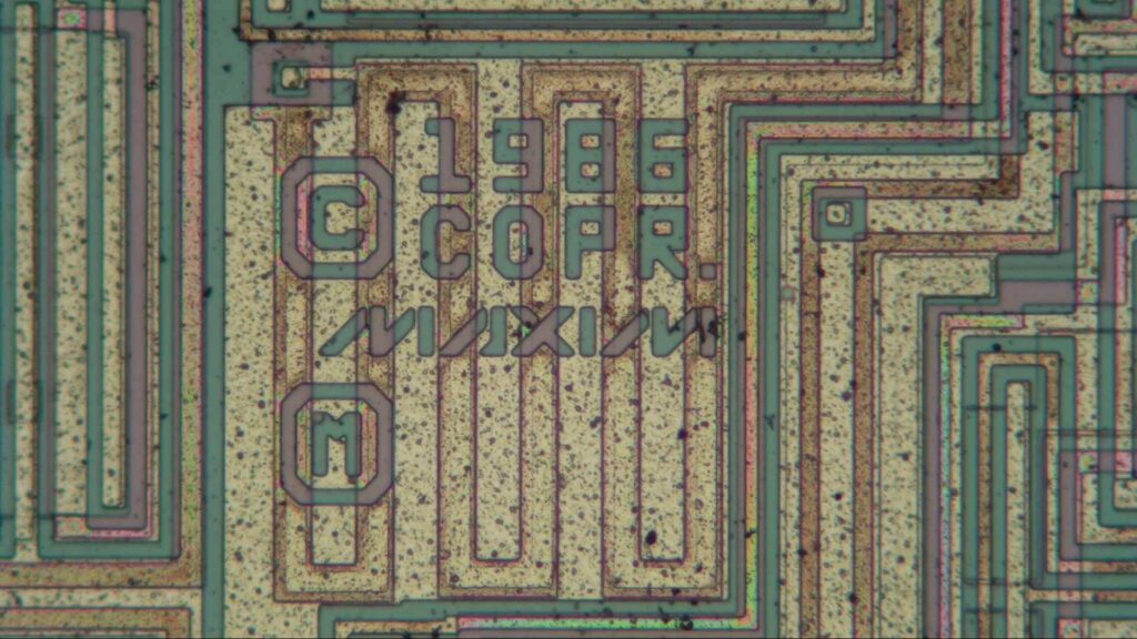
A small 1986 copyright message in the middle confirms we’re looking at the very first generation of this chip.
The datasheet also has an interesting instruction telling us to “connect substrate to V+”. This means that the substrate (the base material in which the transistors are fabricated) is made of n-type silicon. All PMOS transistors are manufactured by implanting p-type diffusions into the substrate, while NMOS transistors are formed through n-type diffusions inside a p-well. A direct result of this is that all PMOS transistors necessarily have their bulk terminals connected to V+, while for NMOS transistors the bulk terminal can be connected to any voltage lower than V+.
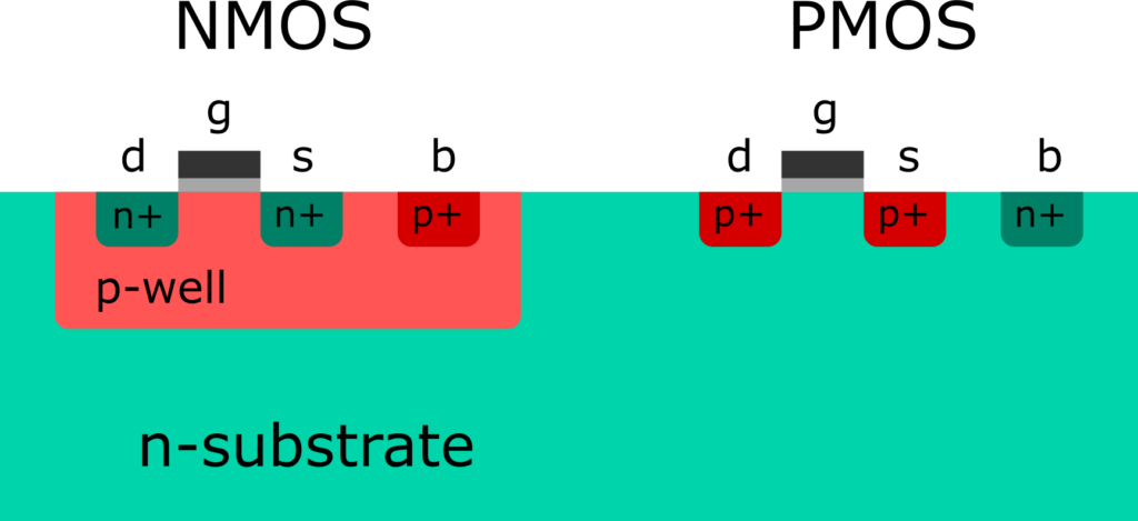
Nowadays it’s far more common to have a p-type substrate with n-wells. The substrate is then connected to the lowest supply voltage (typically GND), and all NMOS transistors share a common bulk terminal. Modern processes (meaning most from the ’90s onwards) even have twin wells, in which each transistor type has its own well, allowing for even more design flexibility.
The MAX232 die can be divided into several functional blocks. On the left is the charge pump, which converts the single +5 V supply into a dual +/- 10 V supply for the two transmitters. Next to the charge pump is a gate driver circuit that applies the right signals to the gates of the charge pump’s power transistors. In the middle we find an oscillator that generates a 20 kHz square wave, next to a bias block that makes a few reference currents. Finally, we find the two transmitters and receivers on the right.
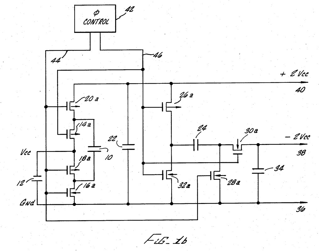
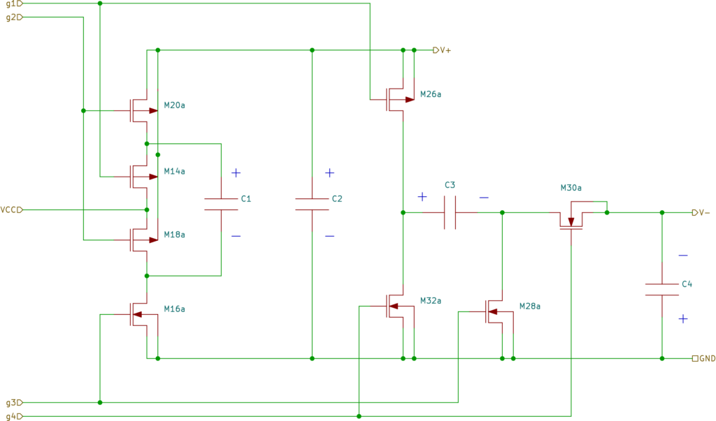
Let’s zoom in on the charge pump first. Dave Bingham and Charles Allen helpfully described their design in US Patent 4636930, which includes the circuit diagram below. It changes the main 0-5 V supply voltage to a symmetrical +/- 10 V supply for the RS-232 drivers.
If we look closely, we can find all eight transistors in the charge pump block. The four on the top (14a, 18a, 20a and 26a) are PMOS devices, while the bottom four are of the NMOS type.
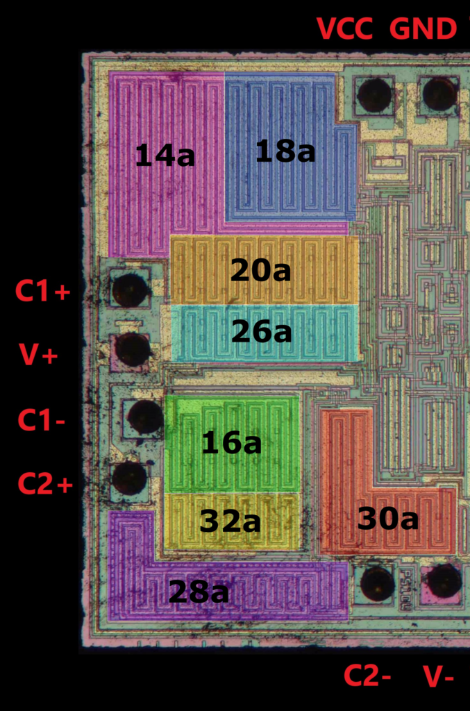
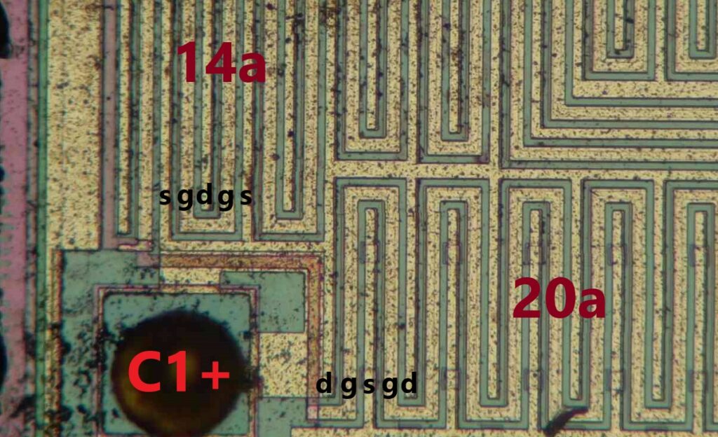
Each transistor has source, drain and gate terminals arranged in a long, serpentine layout such that the drain, gate and source terminals alternate from left to right. I’ve indicated the terminal names for PMOS transistors 14a and 20a below. Note that simple MOS devices like this are completely symmetrical: the drain terminal might as well have been the source and vice versa. In this case I’ve chosen the names based on which direction the current flows when the device is on. Terminal C1+ is therefore connected to the source of 14a and to the drain of 20a.
If we follow the gate lines, we find that the MAX232 doesn’t exactly correspond to the schematic as drawn in the patent. Instead of just two gate signals (labelled 44 and 46) we’ve got four. I’ve drawn a new schematic to show the exact connections, in which I’ve called them g1, g2, g3 and g4.
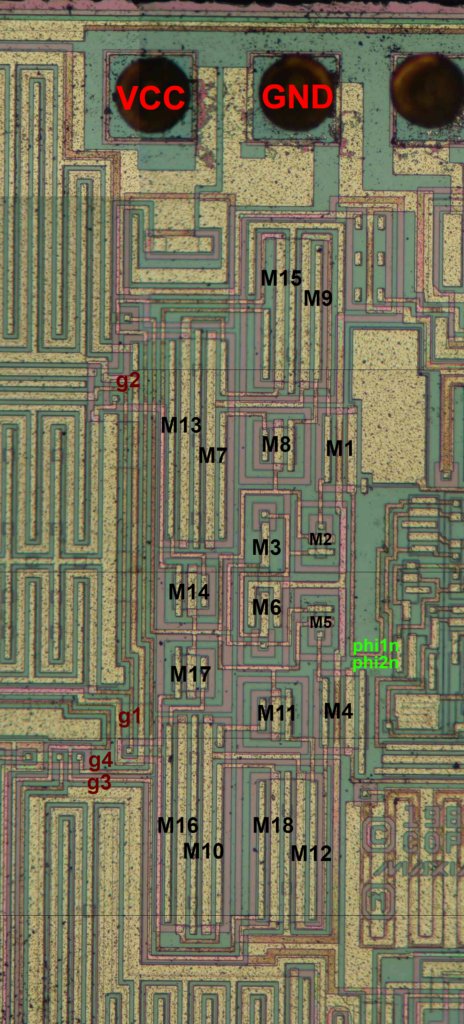
Those four gate signals are generated by the gate driver circuit. It’s a long, slender block in the middle of the chip.
Its schematic isn’t too complicated. There are four inverters, connected between the +/- 10 V supply pins, that each take care of one of the gate signals. They receive their inputs from a level-shifting latch formed by M1-M6, which shifts the input signals (phi1n and phi2n) from 0-5 V to +/- 10 V.
The output transistors of this stage are short and very wide, to give them a large current driving capability. M3 and M6 however, are long and narrow. This means that they drive very little current when they’re turned on, which makes it easy for M1 and M4 to overrule them and toggle the state of the latch.
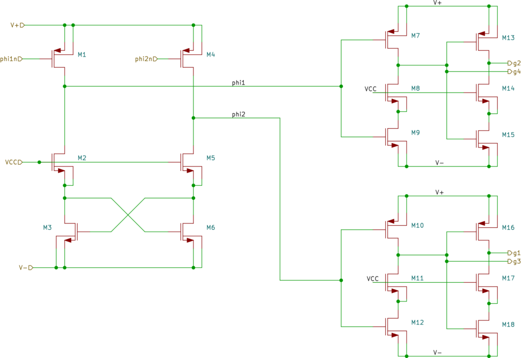
What’s interesting to see is that each branch of this schematic contains an additional NMOS transistor with its gate connected to VCC (M2, M5, M8, M11, M14 and M17). I’m not sure what their purpose is; my guess would be some sort of protection to ensure the charge pump is always functional even if there’s some unusual voltage on the external capacitors during start-up.
One other weird feature of these NMOS transistors is that their gates are connected to this little point right next to power transistor 18a. Apparently that was the most convenient spot to connect to VCC (which is connected to power transistor 18a’s source, the thick vertical wire to the left of the point).
The gate driver’s input signals are generated by an oscillator, which we find right in the centre of the die. It’s a compact circuit made of small transistors, with a single large capacitor at the top.
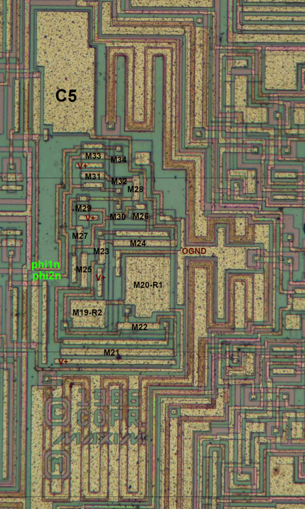
Its basic design is a ring oscillator, with its frequency mainly determined by the two resistors and the capacitor. There’s also a cross-coupled inverter latch (M27-M30) to stabilise the frequency and make it less dependent on transistor threshold voltages. The two resistors R1 and R2 are not separate devices, but are formed by giving M19 and M20 a very long gate length. Both transistors are completely covered with metal (connected to phi2n), but you can still see the meandering gate underneath if you look closely.
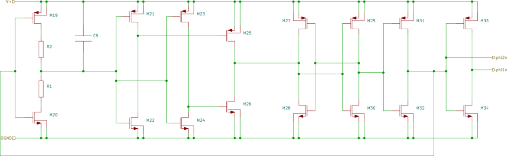
You’ll note that the ground wire of the oscillator isn’t just GND, but a different net which I’ve labelled OGND. We can see what happens to OGND in the bias block:
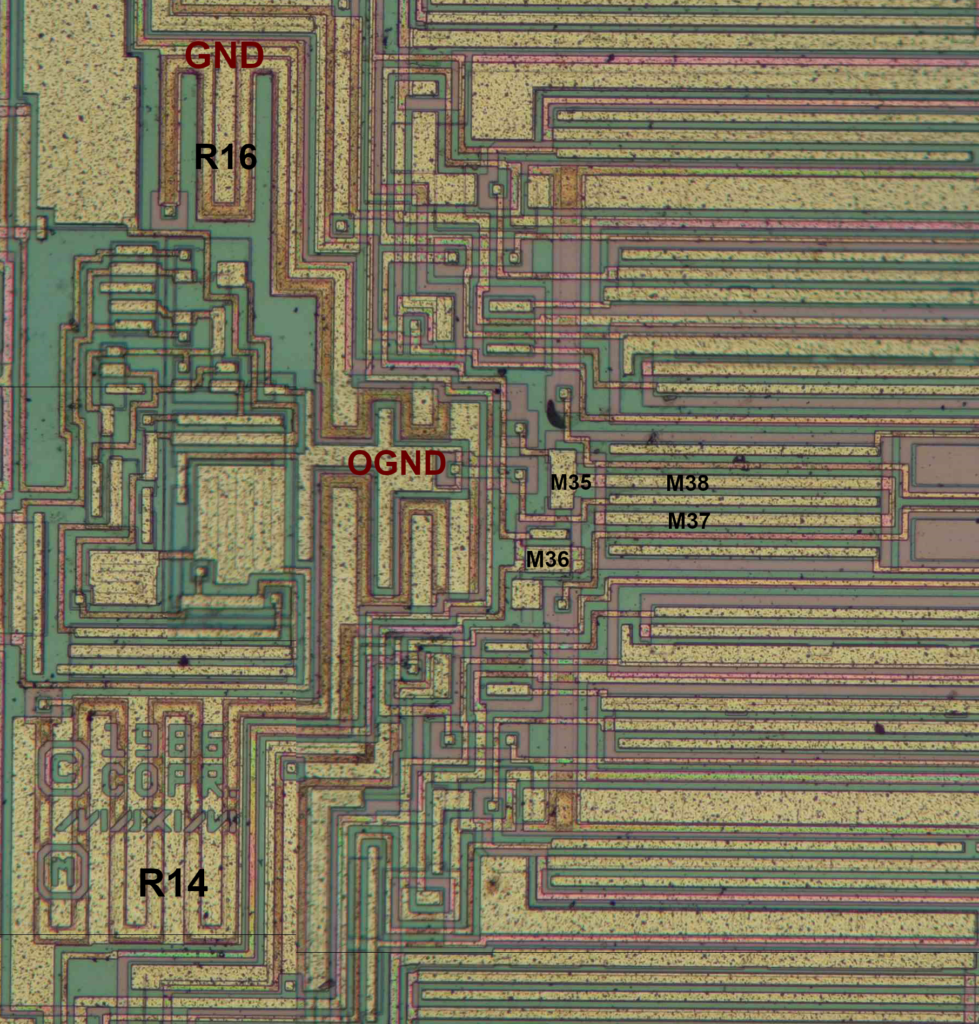
OGND is connected to a long, meandering resistor R14 that eventually connects to GND. There are also a handful of transistors connected to this net to form the following schematic. It looks like R14 is added to limit the oscilator’s supply current and probably slow it down a bit. M36 is a diode-connected PMOS that’s used to generate a PMOS bias voltage used in the receiver and transmitter circuits. M35-M38 do a similar thing, but generate two bias currents that are only used in the two transmitters.
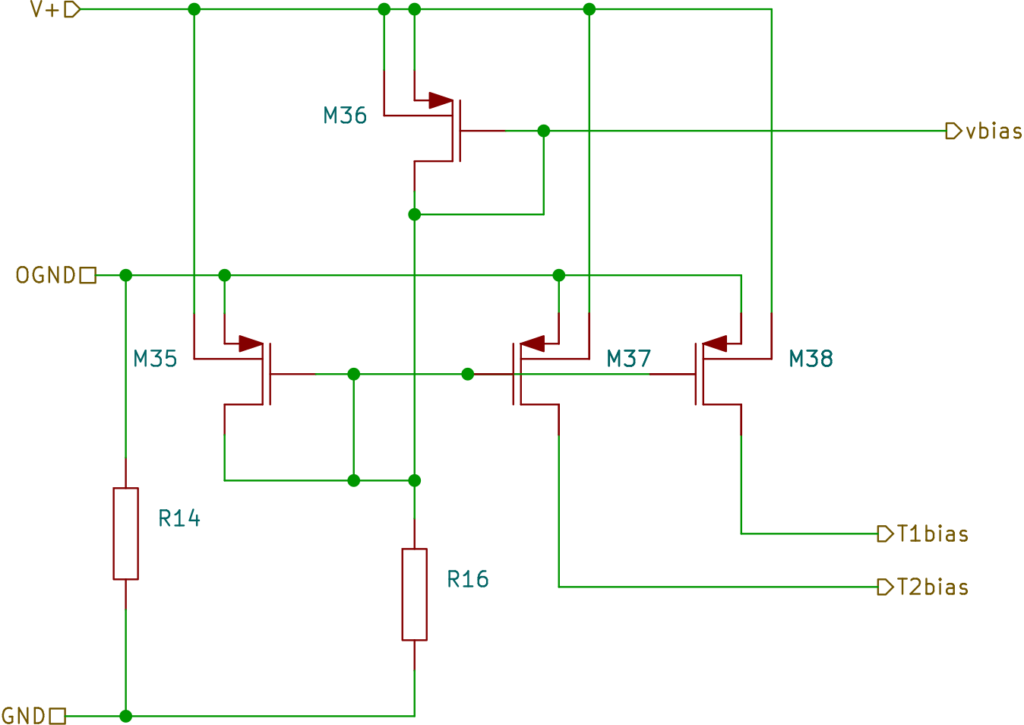
Zooming in on the bit in the centre, we can properly appreciate the weirdness of this circuit. On the left is OGND, which connects to the end of R14. The drain of M37 and M38 also connects to this point, with a bit of space in between to let three wires pass in the vertical direction. It looks weird to me to connect a noisy oscillator circuit to a bias node like this: normally you’d want to keep these two circuits separated as much as possible.
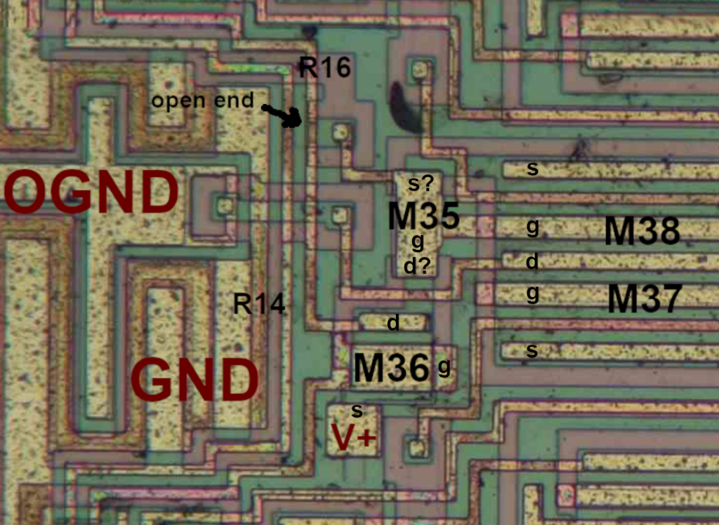
M36 clearly has its gate and drain connected and has a V+ substrate tap below. M35 looks especially unusual: it straddles the drain areas of M36 and M38. Its gate is pulled to GND by R16, which also looks quite odd: its end point is open on the left, unlike all other resistors we see in this picture.
I’m not 100% sure my schematic for this part is correct, but it’s what the layout looks like to me. If you’ve got a better interpretation, please let me know!
Next, we’ll take a look at the RS-232 transmitter. Its input pin is on the right edge of the die, while its output is at the top (not shown here). There is a resistor connected between the output pad and the transmitter’s output signal T1out.
If we trace the schematic, we find a basic CMOS comparator (M39-42) that compares the incoming signal to a reference formed by R4, R15 and R17 together with the current being drawn by M38 (in the bias circuit). The result of the comparison is fed to the output stage, which has a regular NMOS pulldown path and an NPN bipolar pull-up path. In CMOS technology it’s easy to make a reasonably good bipolar transistor with its collector connected to the substrate, which will have much higher current capacity than a similarly-sized MOS transistor.
The diagram below shows what such a vertical NPN looks like: an n+ diffusion forms the emitter, a p-well becomes the base, and the n-substrate acts as the collector.
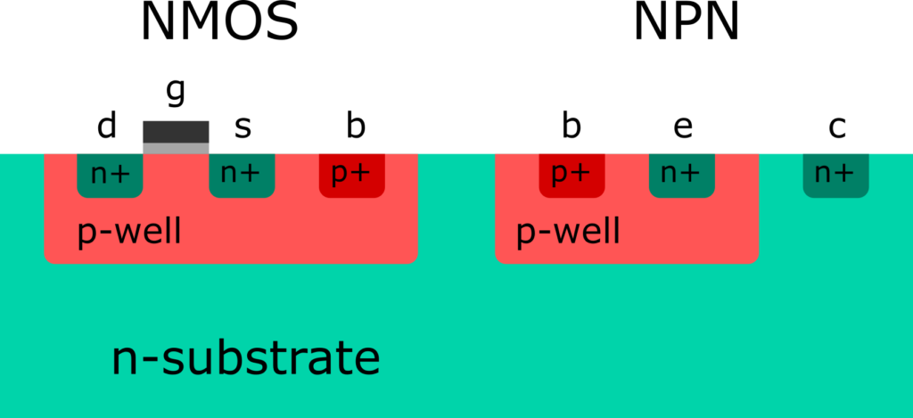
In CMOS processes that use a p-type substrate, all polarities are reversed and you end up with a vertical PNP instead.
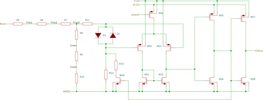
Finally, we’ll check out the receiver. One striking feature of this circuit is the input resistor, which is made as a long, winding piece of polysilicon. There are several test pads next to it which allow the manufacturer to adjust the resistor’s value after production. A high voltage is applied between two test pads to zap the little piece of wire that connects them, creating an open circuit.
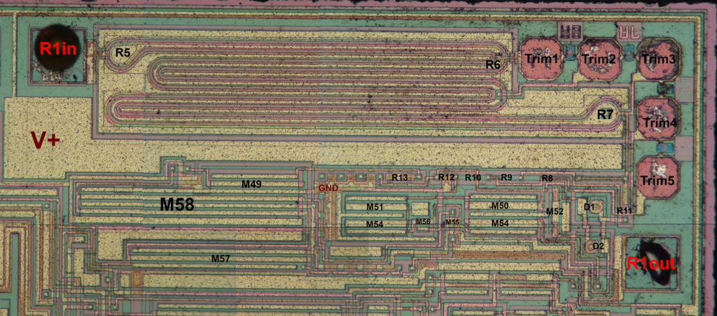
The schematic looks surprisingly similar to that of the transmitter. We’ve got a CMOS comparator again (M50-M54), but this time with a full CMOS output stage (M55-M58). The input voltage is compared to a version that’s been clamped against GND by D1 and D2, with a bit of hysteresis through M49. The whole resistor chain on the input side is designed to give the chip an input pull-down resistance close to 5 kΩ as described in the datasheet.
So there you have it, a complete schematic of the classic MAX232. It’s been really interesting diving into the circuitry of this famous chip and figuring out what makes it tick; the components on ancient CMOS devices like this one are large enough to clearly see with a simple microscope, but they often use weird layout tricks that take a while to figure out.