The Raspberry Pi Pico is the latest in the Raspberry Pi series of single-board computers. Introduced in January of 2021, the Pico marks a significant change from the earlier series: instead of having a Broadcom system-on-chip, the Pico’s heart is a custom IC with a dual-core ARM Cortex-M0 processor at 133 MHz. Combined with its tiny form factor and lack of interfaces like HDMI, it feels more like a supercharged Arduino than a small PC.
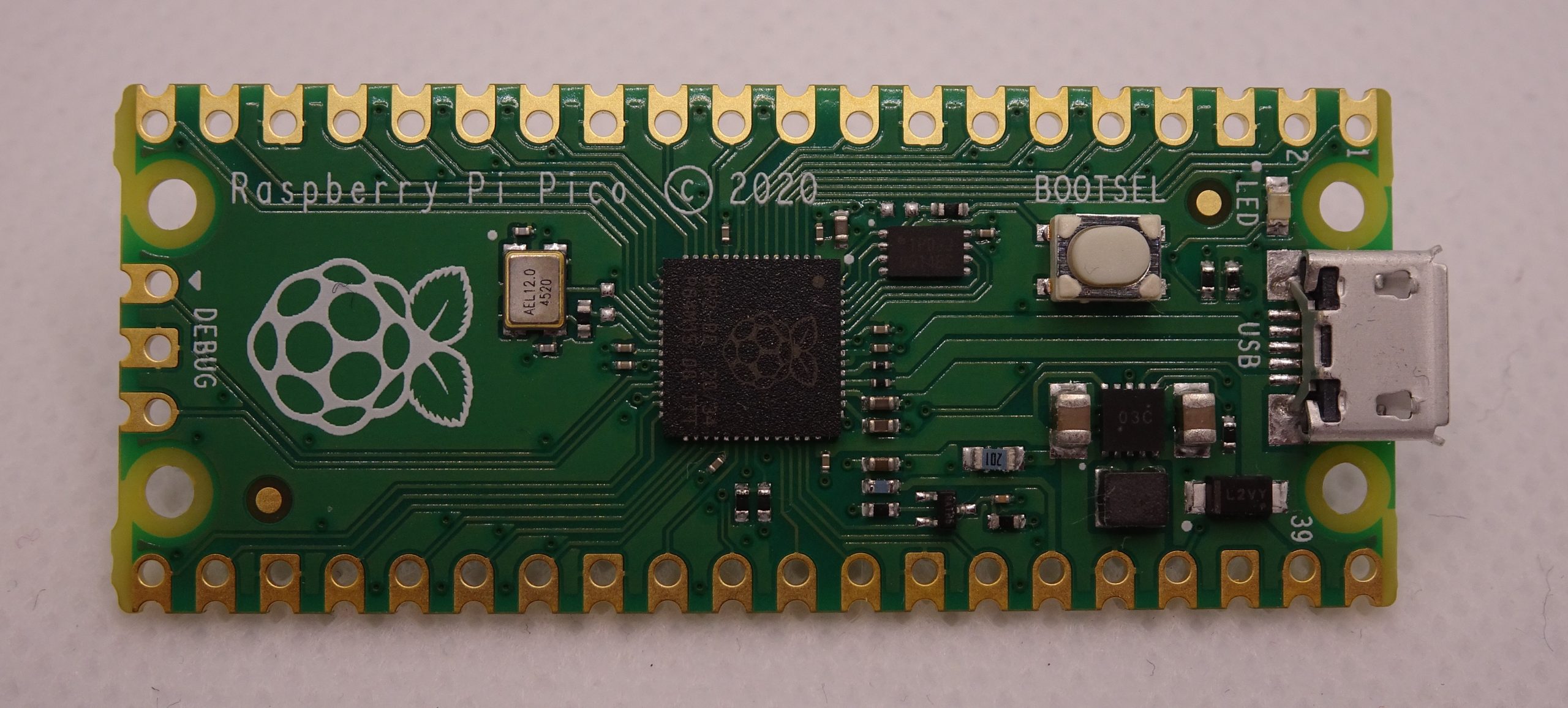
This is the Pico. It contains the main CPU in the centre, 16 Mbits of flash memory next to it, a DC/DC converter on the right, and a USB connector to program the whole thing. I/O pins are scattered around the edge to enable easy interfacing to its environment.
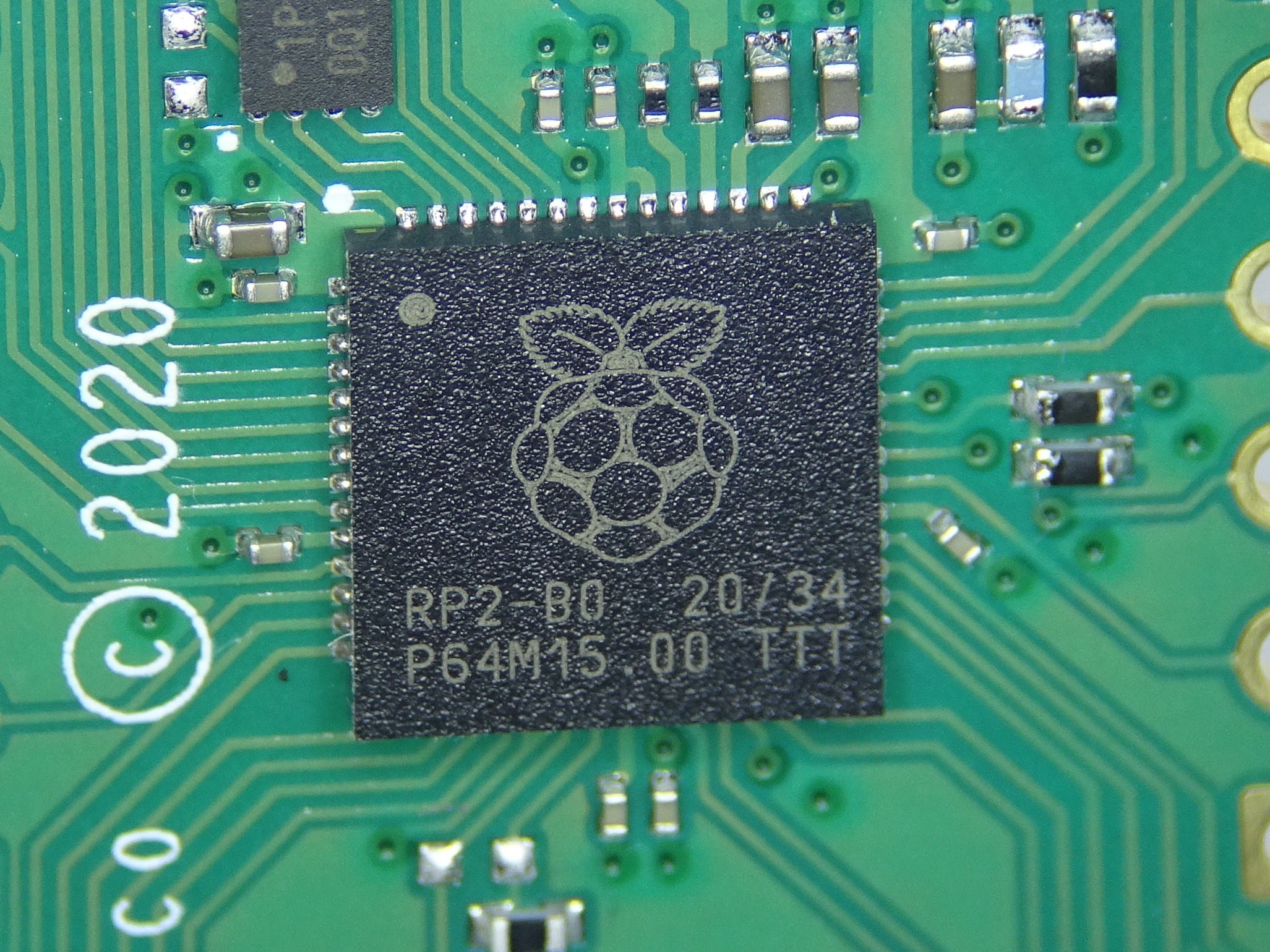
The main CPU is the RP2040. Apart from the dual-core processor, it contains 264 kB of RAM, a four-channel, 12-bit ADC, 30 GPIOs, plus your standard timers and bus interfaces. All of this squeezed into a 56-pin QFN package measuring just 7×7 mm.
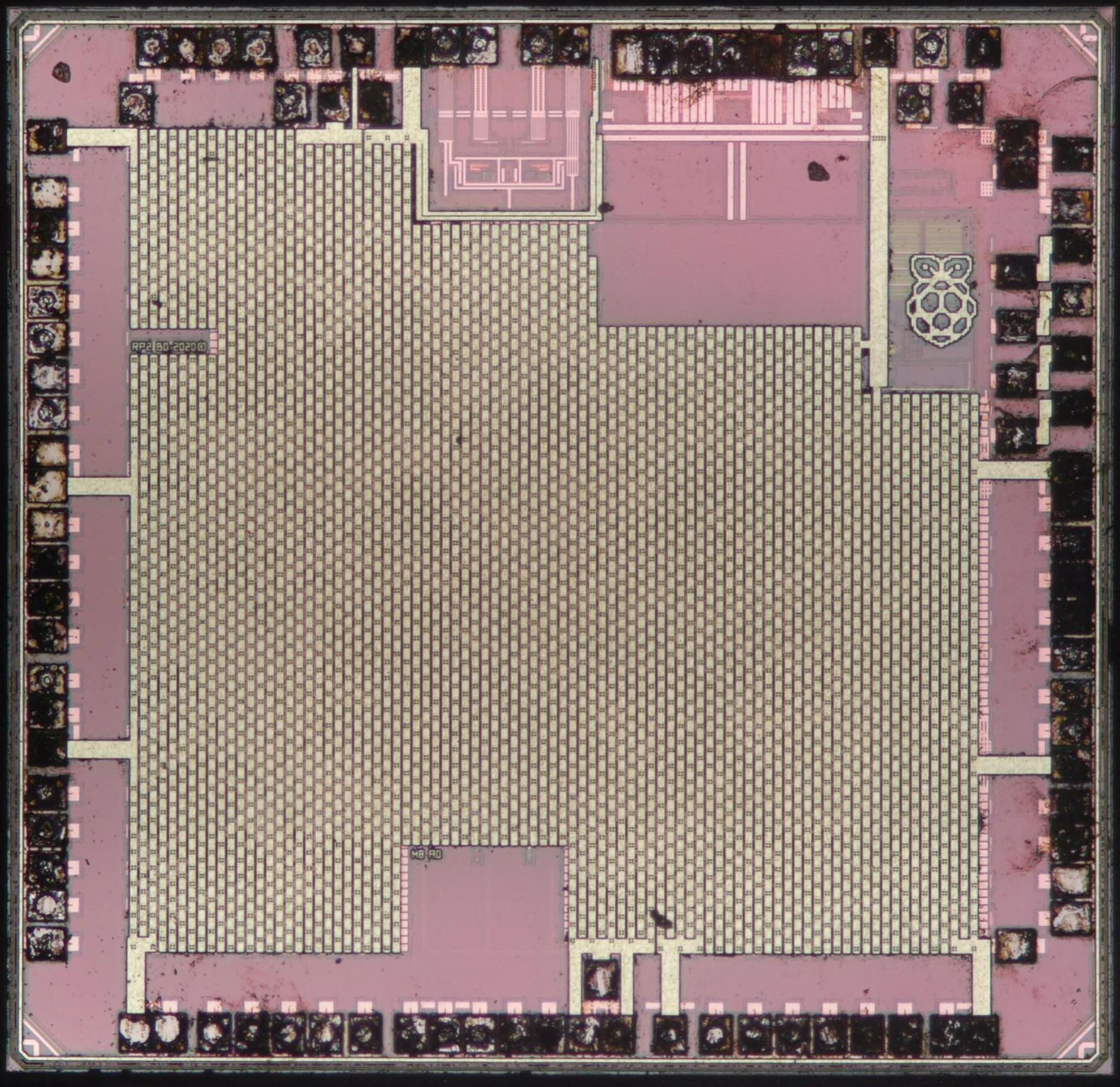
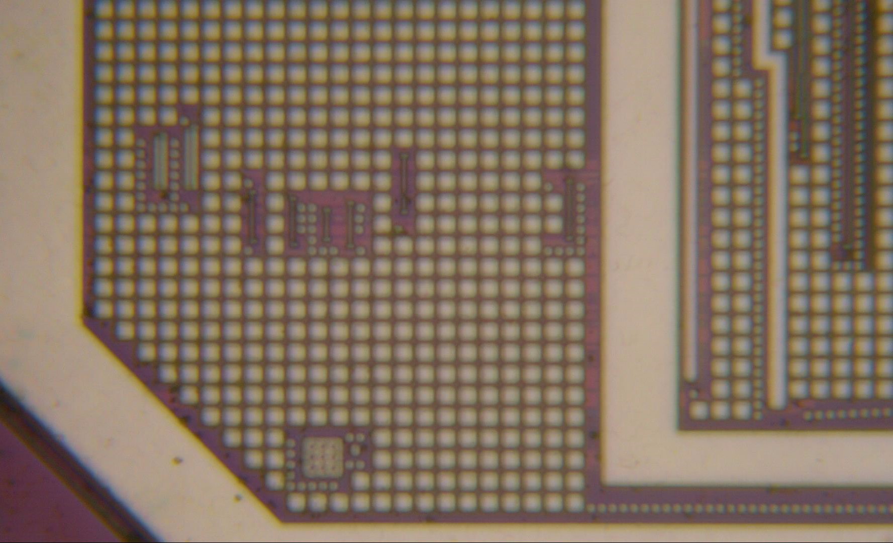
After opening up the package we run into what looks like a huge brick wall. Most of the die is covered by a repetitive pattern on the top metal layer: this is the power distribution network, ensuring a low-resistance path from the supply pins to every part of the chip. Most likely there is only digital circuitry below this pattern. At the top-right corner we find the Raspberry Pi logo with the ADC below it. To the left of that we find the voltage regulator that generates 1.1 V to power the processor cores. Finally, to the left of the voltage regulator are the nicely symmetric circuits that power the USB interface.
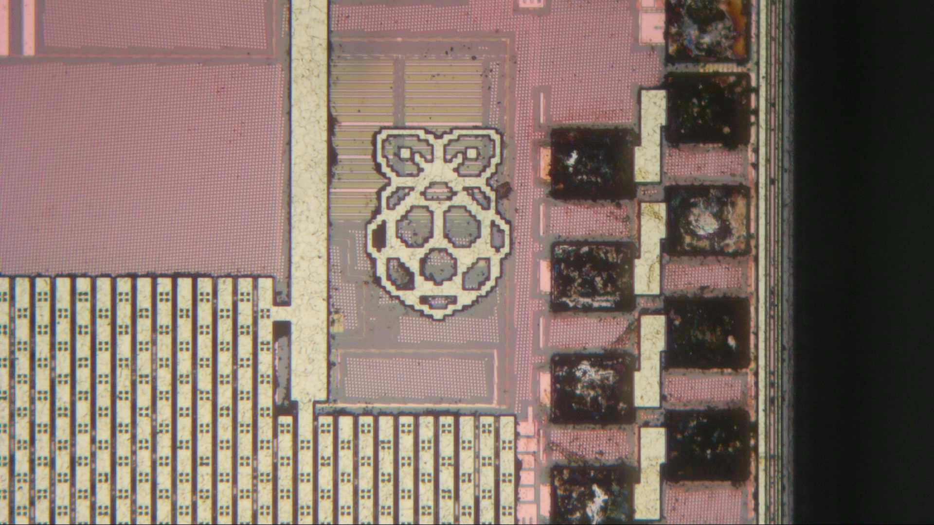
The Raspberry logo covers the ADC, and to the right we find the four analog input pins. It looks like these pads are double-bonded, using two bond pads per pin connected by an S-shaped metal line.
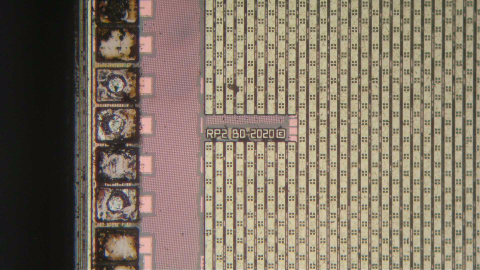
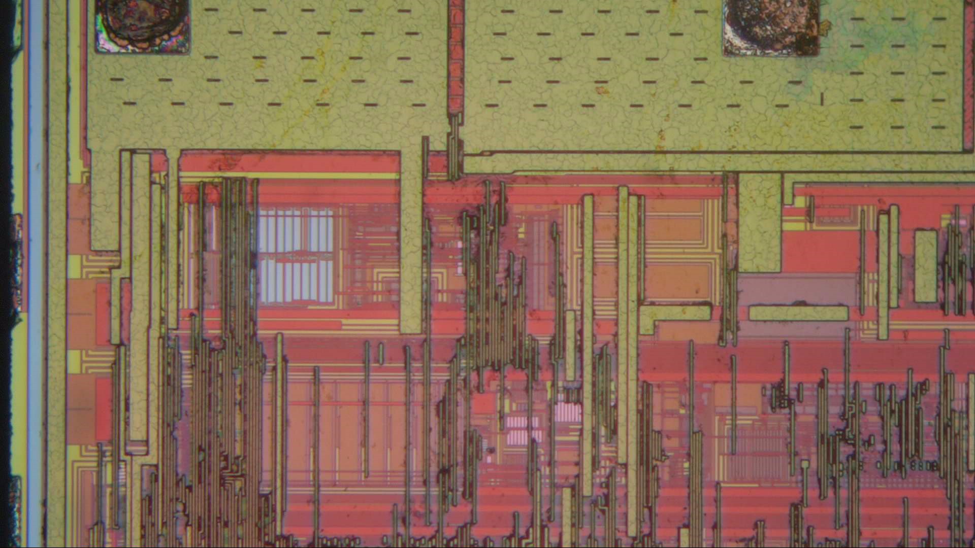
At the left edge we find the 2020 copyright date and the identifier “RP2 B0”.
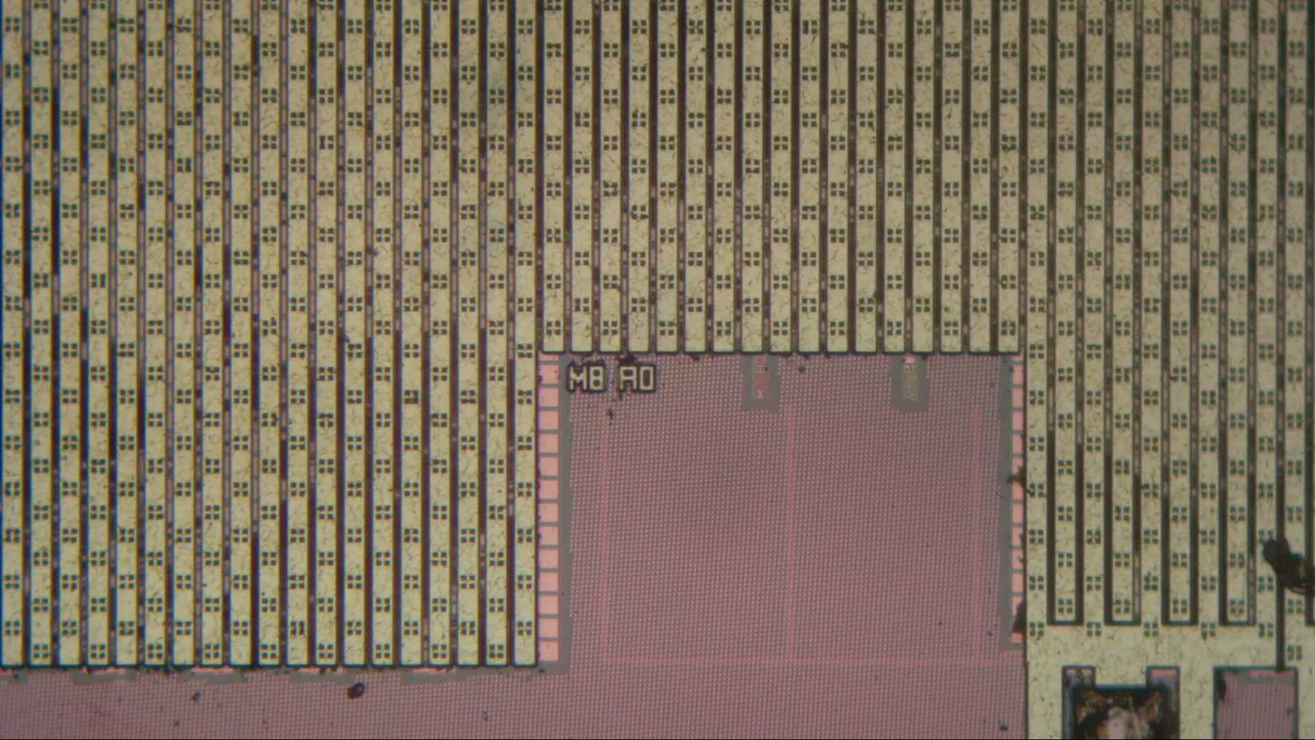
On the lower end we find “M8 A0”. At first I thought these were someone’s intials, but actually this is a revision letter for the top metal layer, M8. This chip is made in TSMC’s 40 nm process, with apparently eight metal layers.
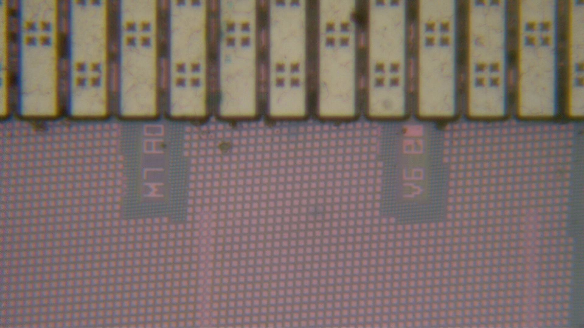
Zooming in a bit more we also find Metal layer 7 and Via layer 6. The tiny squares we see are dummy shapes, placed to ensure a relatively uniform coverage of metal on that layer. Non-uniform metal coverage (for example, having lots of wires on one end of the chip and an empty area somewhere else) can cause problems with etching. Modern IC processes like this have very strict rules on metal coverage, because a very small change in etch rate can cause short circuits in one place and broken connections in another.
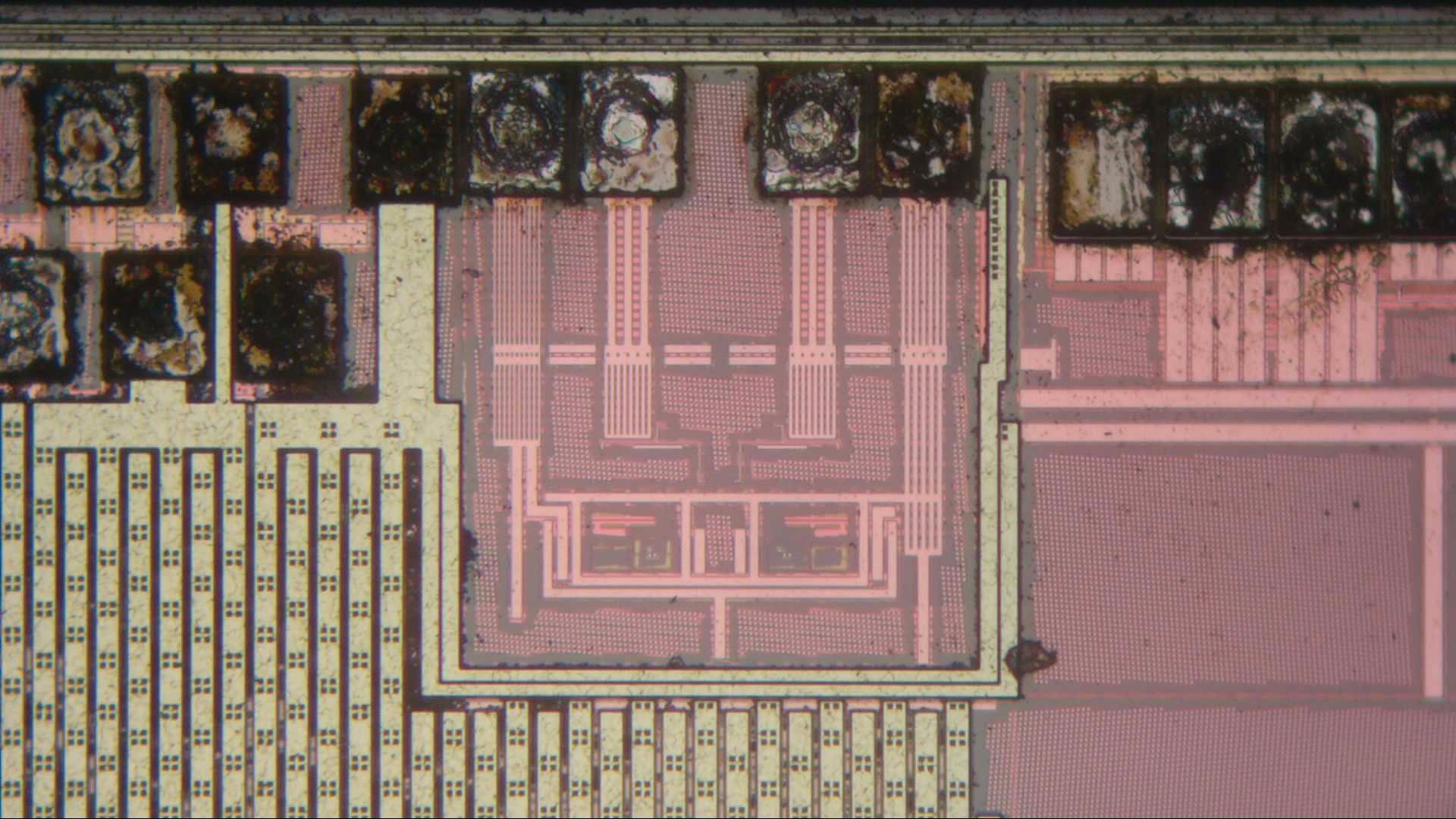
Zooming in on the USB interface driver we find relatively large circuits that can deal with the high voltages present on the bus. The actual circuits are still way too small to see, and much of the layout is obscured by the dummies on Metal layer 6.
Next to the main processor we find the 16 Mbit flash chip, a Winbond W25Q16. This contains all the code that the RP2040 runs; the processor has no flash of its own. A dedicated SPI bus connects the flash to the CPU.
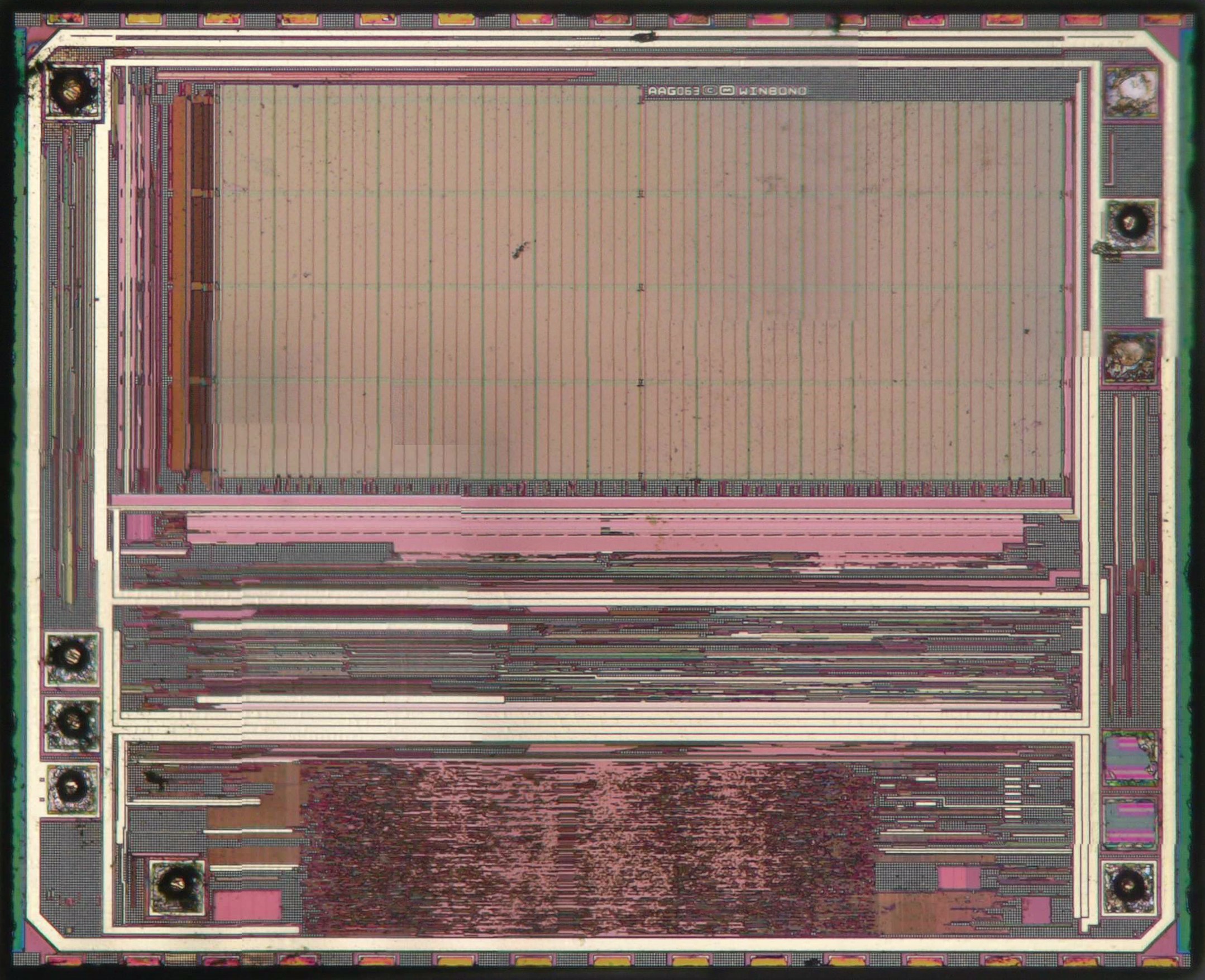
Inside we find a typical memory chip: a large bank of memory cells at the top, decoding logic below it and a small digital core at the bottom.
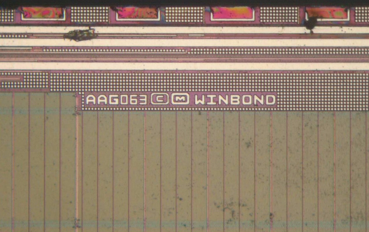
Apparently Winbond calls this chip the AAG063 internally. There is no copyright date, but the corresponding datasheet is from 2014.
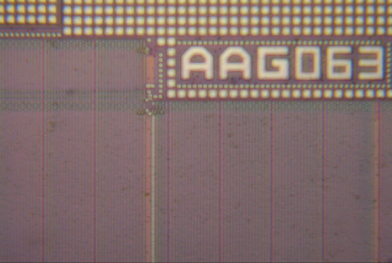
The memory area consists of long vertical lines connecting the columns together. The actual cells are much to small to see. Note how this chip also has lots of dummy squares on the top metal layer.
At the bottom-left corner there are a few spots where the dummy grid has been opened. Probably the circuits below needed to use the top layer for routing a few signals.
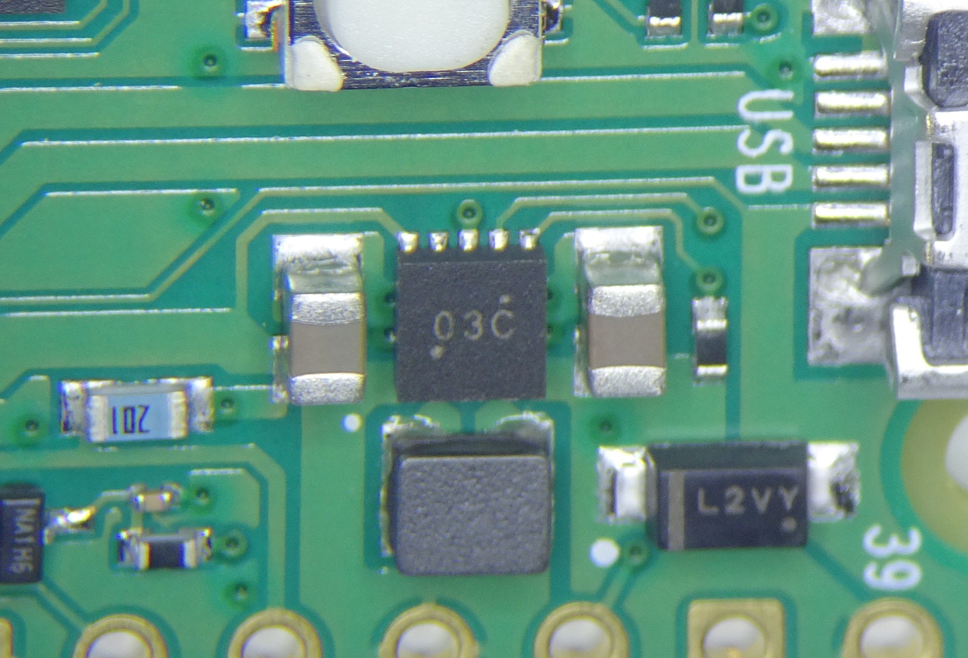
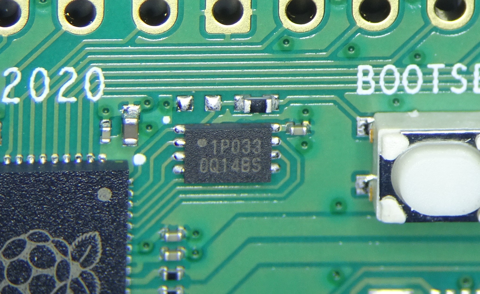
Finally we have the Richtek RT6150B buck-boost converter. It converts the 5 V coming from the USB connection to 3.3 V used by the rest of the system. The chip is surrounded by two 47 uF capacitors and a 2.2 uH inductor.
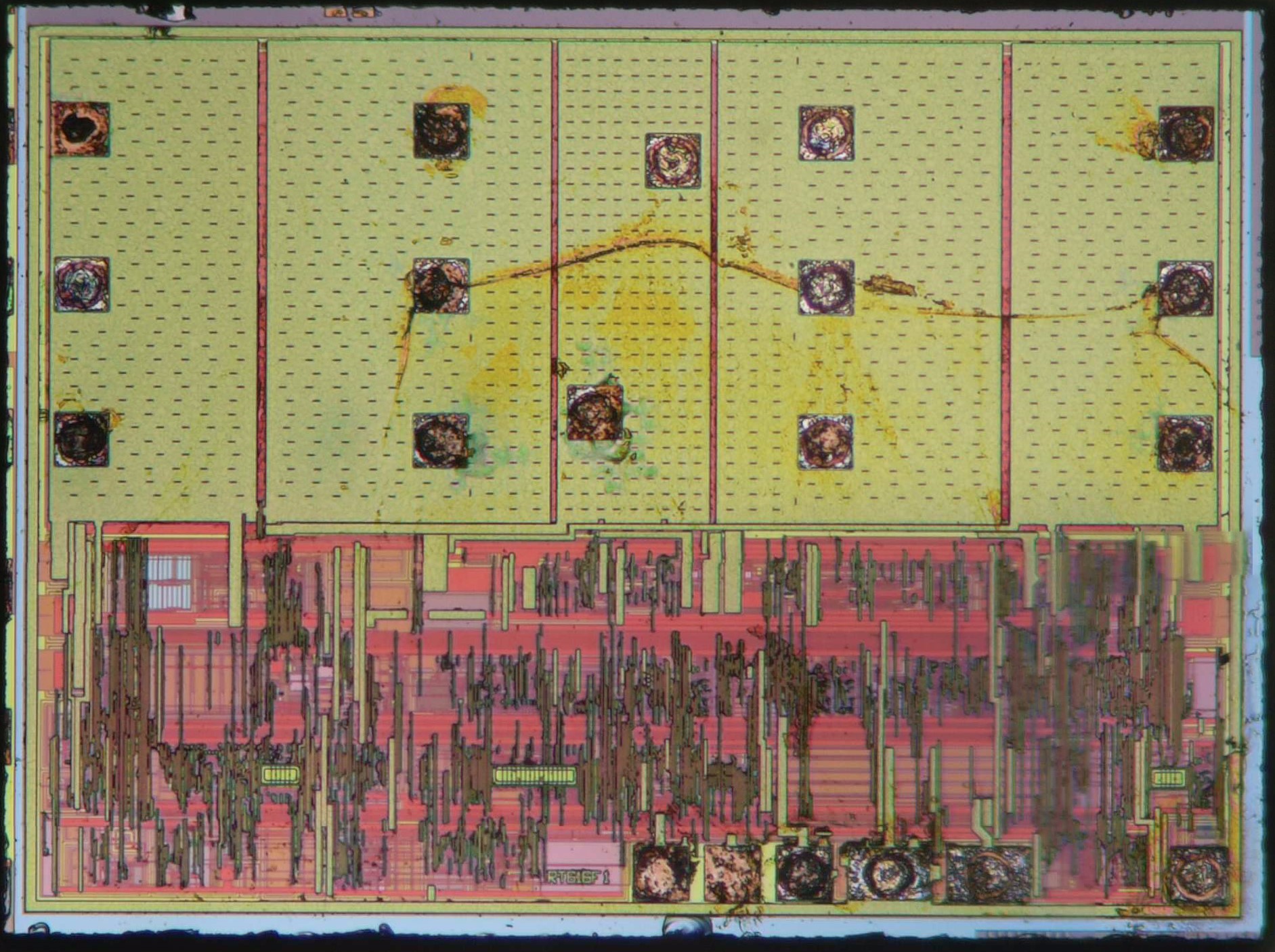
Inside we find more than half of the area taken up by the power transistors. This chip contains two PMOS and two NMOS transistors.The bond pads are distributed evenly across the metal layer covering the transistors, to ensure all currents are also evenly distributed along the transistors’ widths. From left to right, we find pins Vin, Lx1, GND, Lx2 and Vout.The larger PMOS transistors are at the left and right, while the smaller NMOS transistors are in the middle.
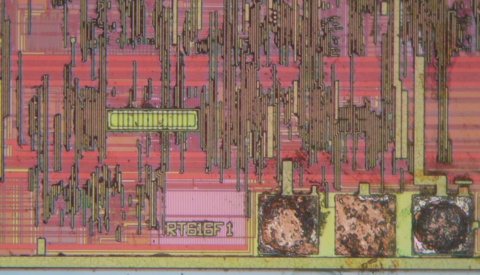
The die identifier is “RT616F 1”. The rest of the chip contains control circuits, which include comparators, an oscillator, current sensors and a temperature controller.
Below the output transistors we can just catch a glimpse of some analog circuits: blue resistors and orange capacitors.
Great job! Thank you for your enthusiasm!
Fascinating to read all these internal details. I assume you acid-etch off the casing and then use a microscope? I’d be interested to know how you get inside the chips.
Hi David! Yes, I use chemical etching to strip off the epoxy package and then look at the internals with a metallurgical microscope.