Most electronic systems that need an accurate clock, which is to say most microprocessor-based systems, use a quartz oscillator. You’ll typically see a metal package somewhere near your chip that contains a slice of quartz which resonates at a certain frequency thanks to the piezoelectric effect.
Quartz crystals are cheap and provide a very accurate clock frequency, but they take up quite a bit of space and are sensitive to shocks. To deal with those two problems, fully on-chip oscillator systems have been available since about 2010. These use micro-electro-mechanical systems (MEMS) technology, which involves the manufacture of tiny moving structures on a chip. Their price is typically higher than that of a quartz crystal however, and their frequency stability and phase noise performance are often a bit worse. Today we’ll have a look at a few different MEMS oscillator chips and see what they look like inside.
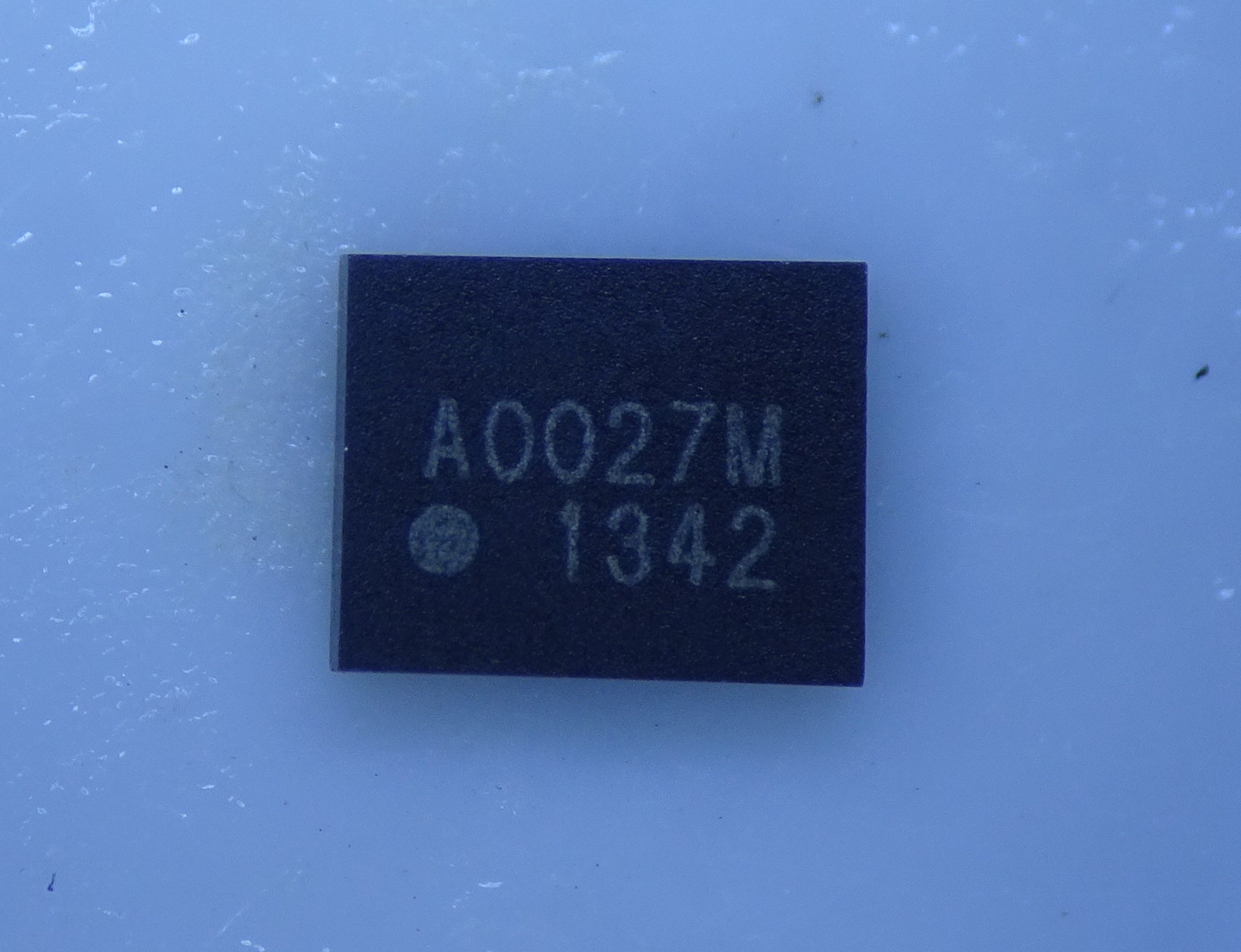
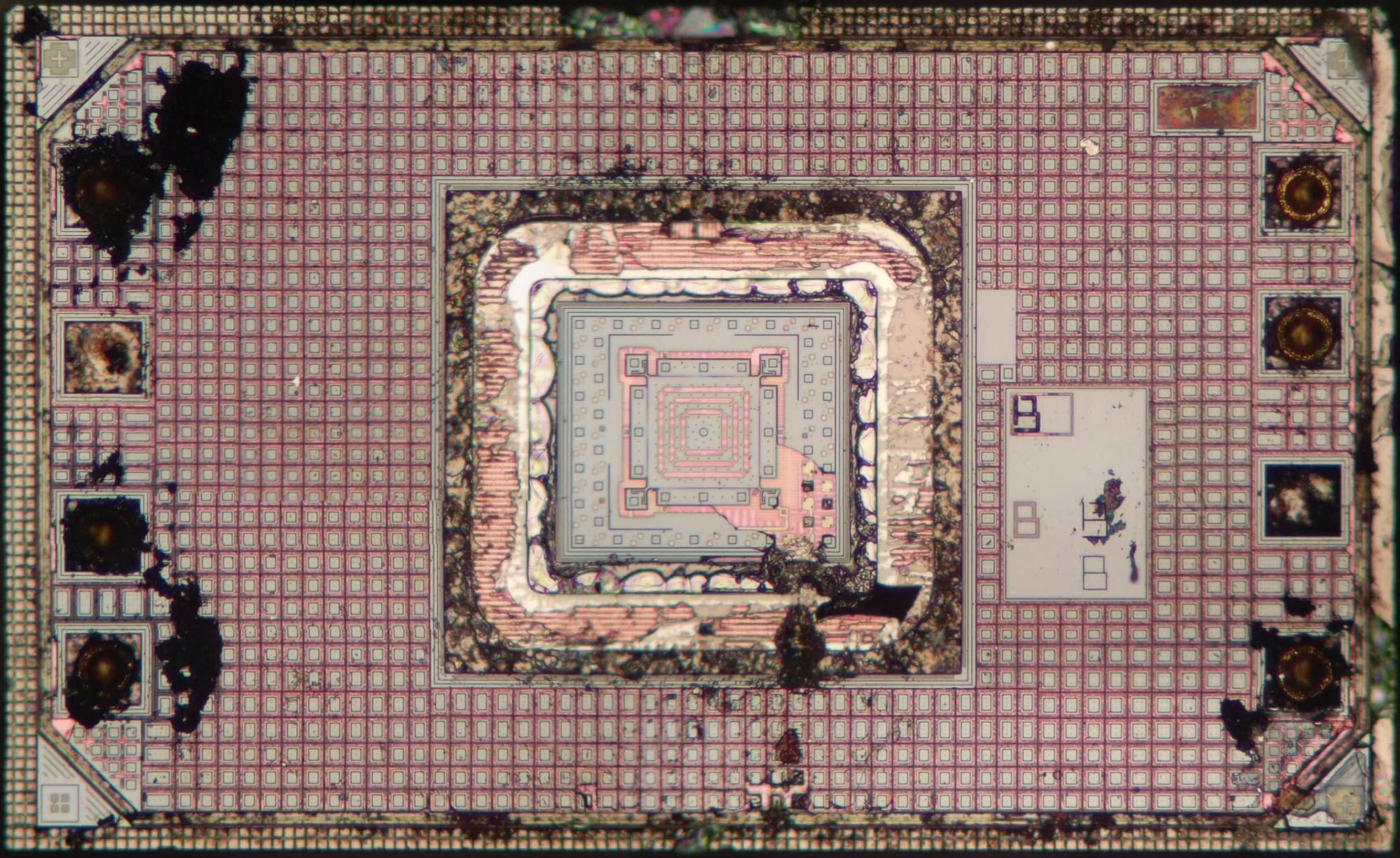
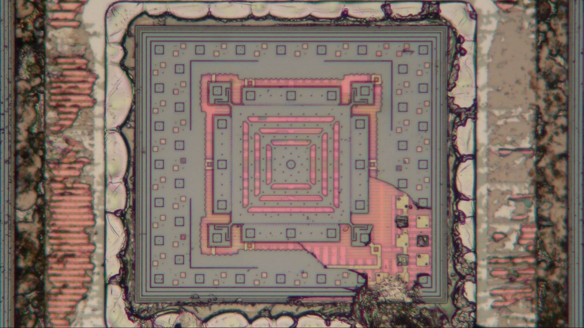
First up is the Si501 by Silicon Labs. It’s an 8 MHz oscillator built using what Silicon Labs call CMEMS technology, which means that they integrate the MEMS bit on the same chip as the rest of their circuits. The package looks rather anonymous, with just a cryptic part number and no manufacturer’s logo. Silicon Labs have since sold their MEMS oscillator business to Skyworks, so future versions of this chip might have a different marking.
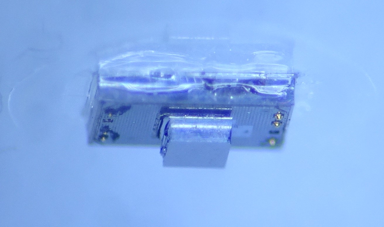
Inside, we don’t see much either. There are two chips, with the main chip at the bottom and a smaller one bonded on top of it, upside-down. The picture below is a combination of two separate pictures, because it’s impossible to get both dies in focus at the same time.
Here you can see how thick the secondary die is. It’s directly bonded to the main die.
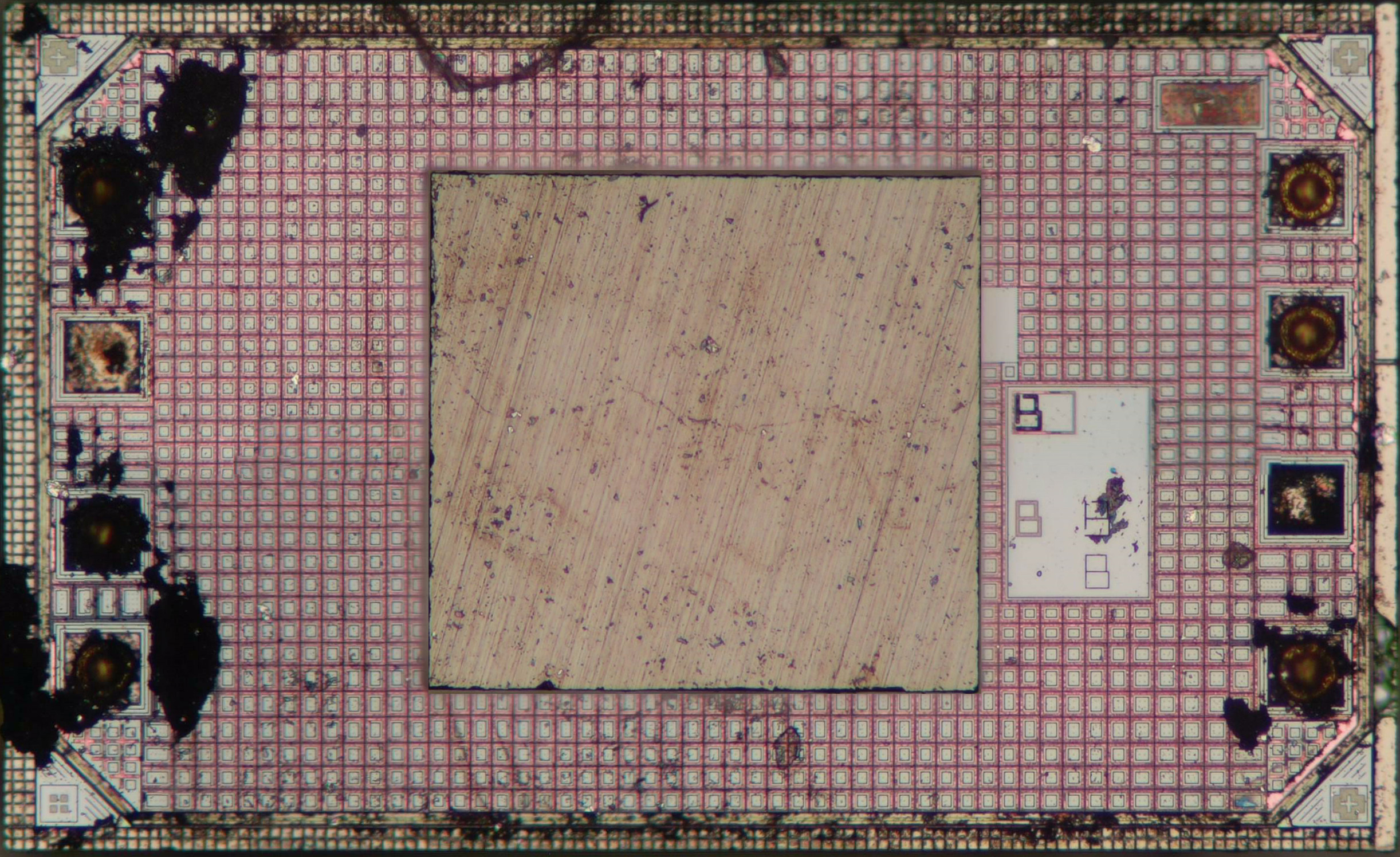
There’s not much to be seen on the larger die: apart from some alignment markers in the corner and a few “B” revision letters, everything’s hidden beneath a grid of some sort.
In this corner we find an alignment marker and an area with a few numbers. It’s kind of hard to make out what it says because of some layer that seems to be disintegrating.
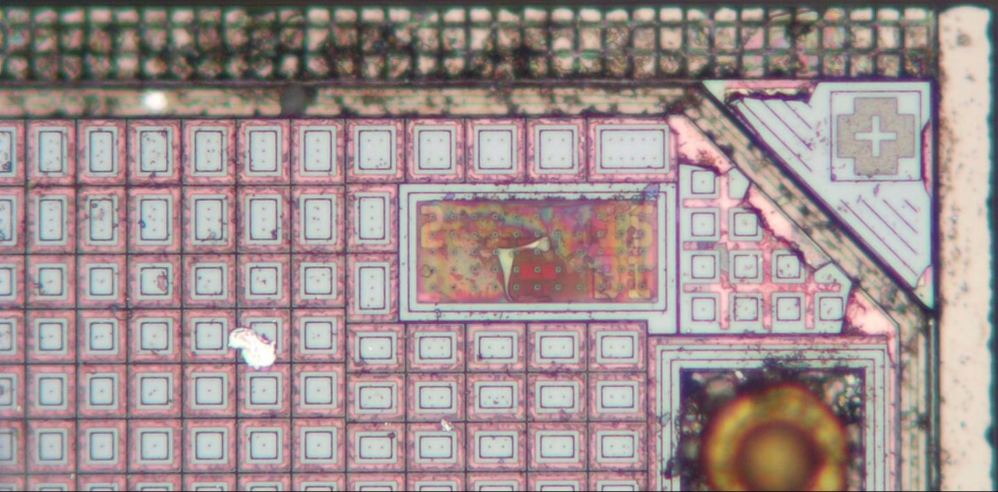
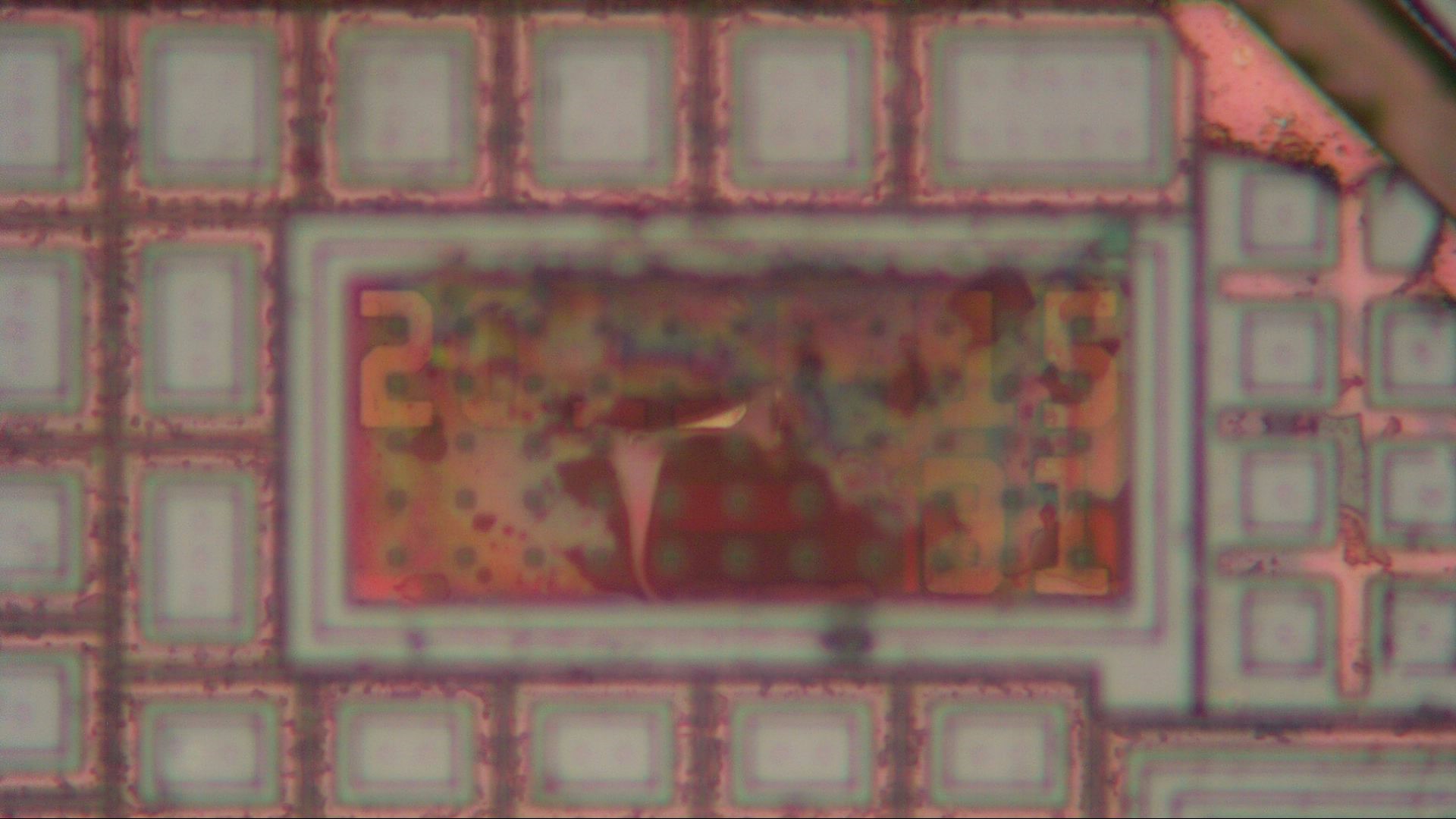
Zooming in a bit more, we can see that it probably says “2013M15 B1”.
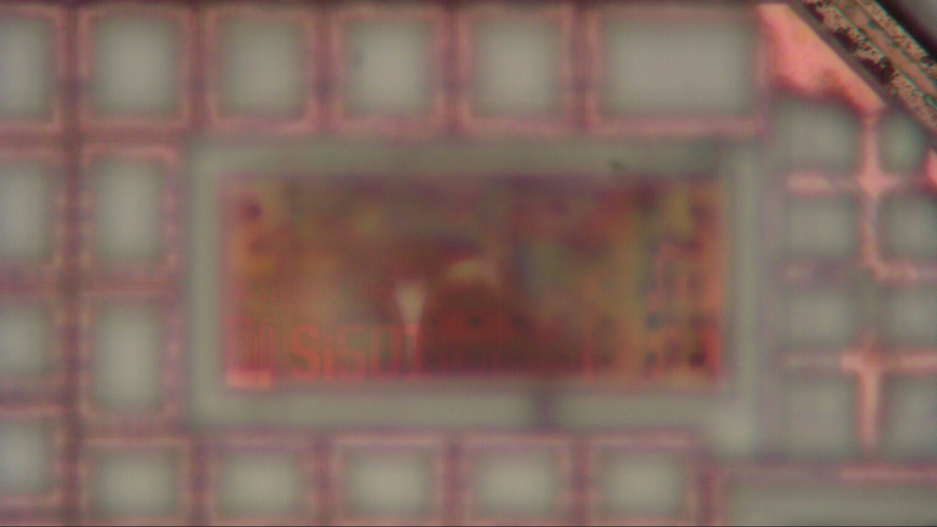
If we slightly change the focus, we can also make out “Silicon Labs Si501”. So at least we’re looking at the correct chip here.
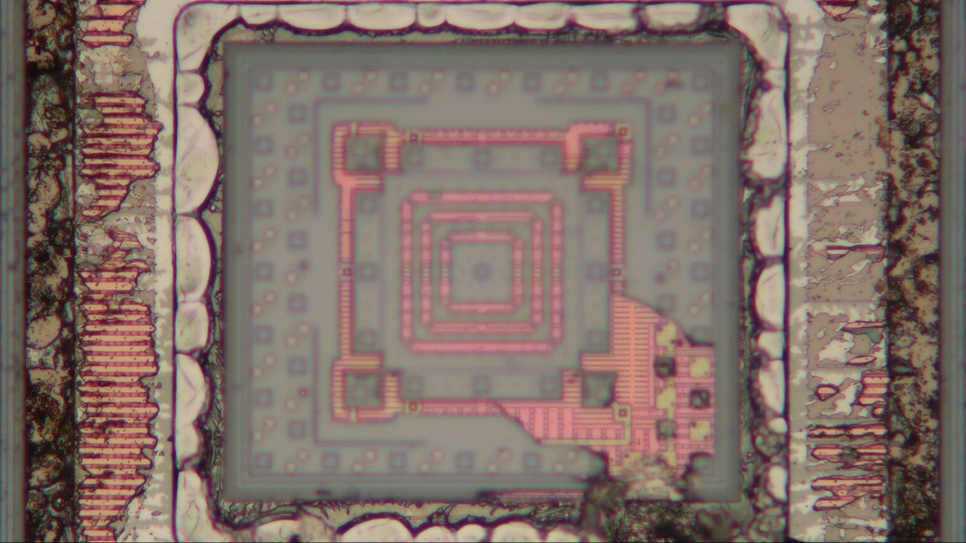
When we take the seconday die off however, things get interesting. The secondary die is just a silicon seal, with the MEMS part integrated onto the main die. As we’ll see, Silicon Labs is unique in this: all the other manufacturers have a separate chip to hold the MEMS devices.
Getting the seal off was kind of tricky: it was bonded very tightly to the main die, probably by some kind of glue, and trying to apply any kind of force onto such a tiny sliver of silicon without crushing it is not easy. In the end, there was a bit of damage to the main die, but we still get a great view of the MEMS core.
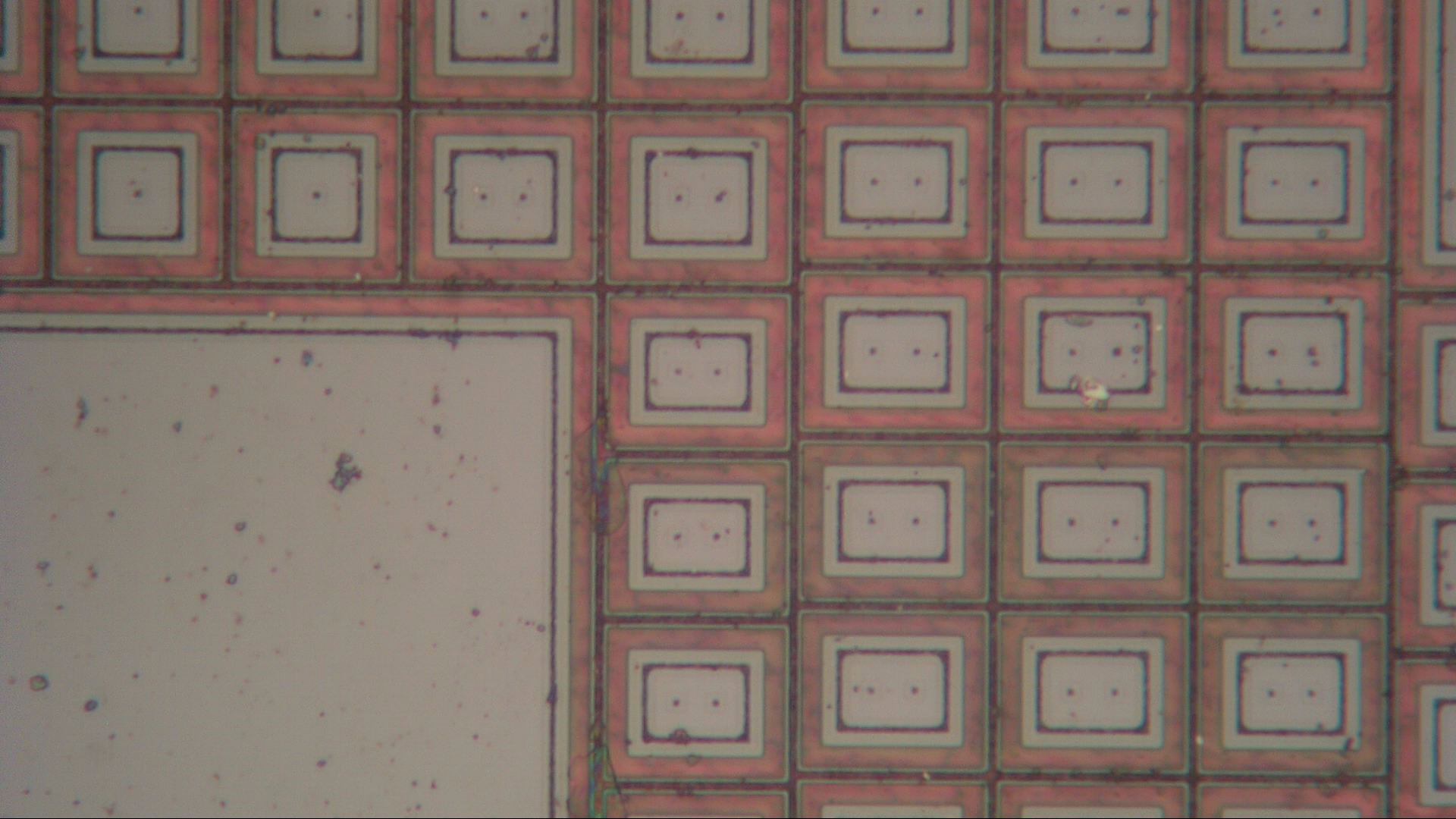
It looks like those squares that cover the rest of the chip are made from the same material as the MEMS layers. Covering the whole chip with such dummy structures is done to keep the etching process under control: first, the whole chip is covered with a layer of metal (or perhaps silicon, in the case of MEMS), which is then etched away in certain places. If the MEMS layers were only used in that square in the middle of the chip, then a huge amount of material would need to be etched away everywhere else. It’s easier for the etching process if most of the material can be left in place.
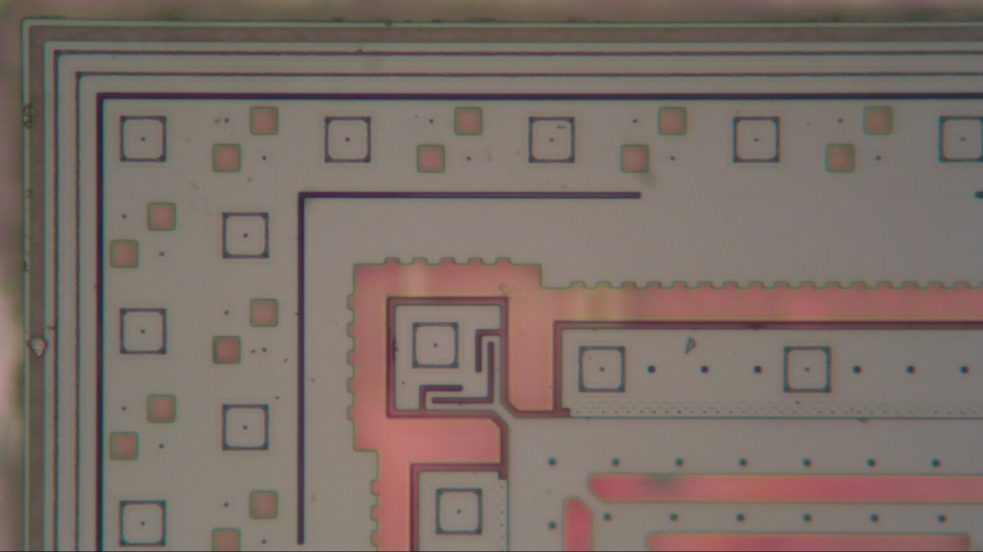
The resonator consists of a square frame that’s attached to the main chip at four points. Those points are flexible, allowing the frame to vibrate. The exact shape is carefully designed to resonate reliably at the desired frequency.
There are lots of interesting shapes below the MEMS structure as well. We can see them more clearly by slightly changing the focus.
The outer frame has a serrated edge, while the hinge that holds the main mass has two little loops to give it additional flexibility. Those squares with a point in the middle are vias that connect the grey layer to the one below.
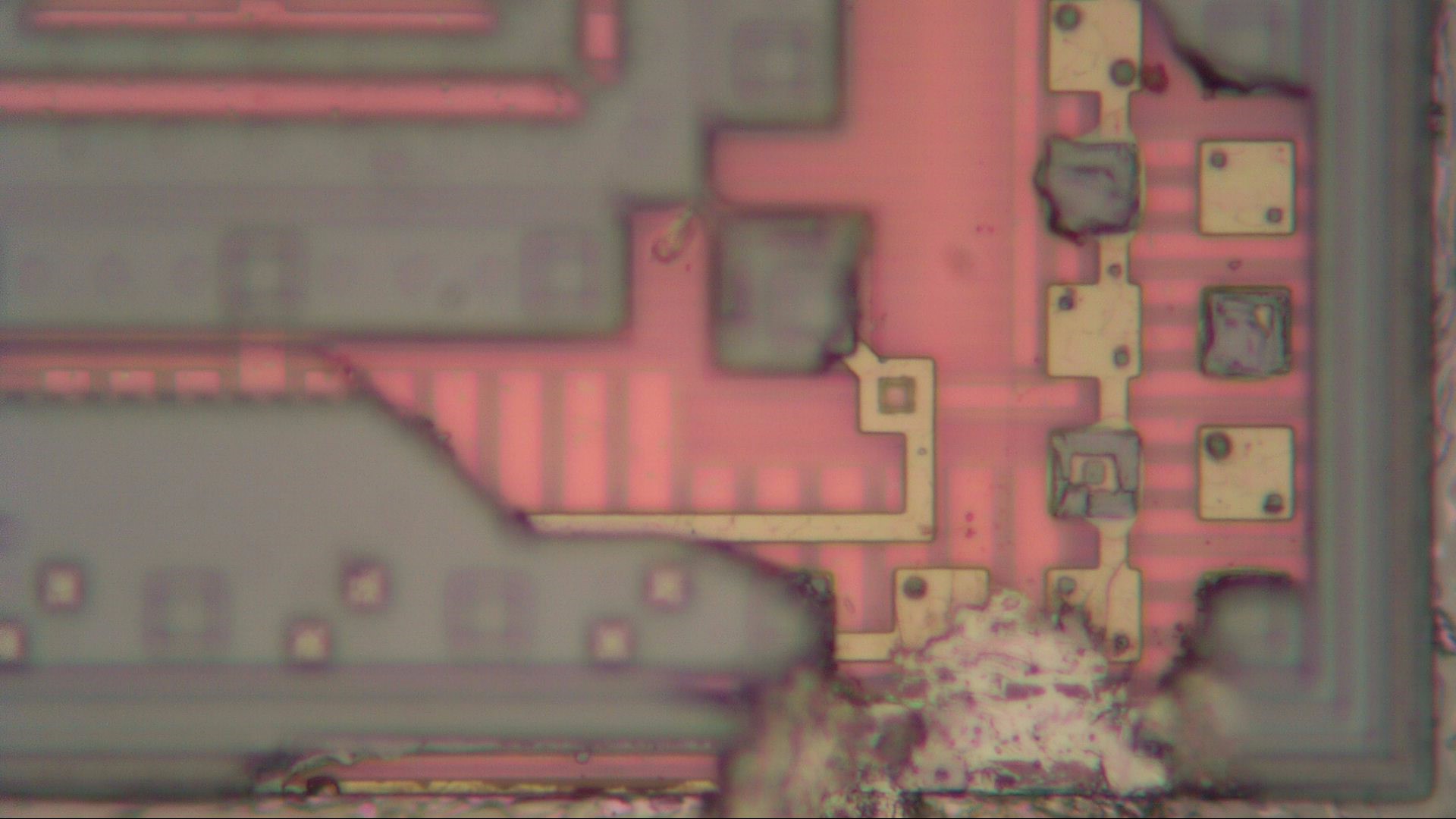
The damaged part gives us a nice view of the lower layers. There is a metal layer (which appears yellow here) that connects to the main mass at this corner. The lower layer connects to the upper layer through square vias.
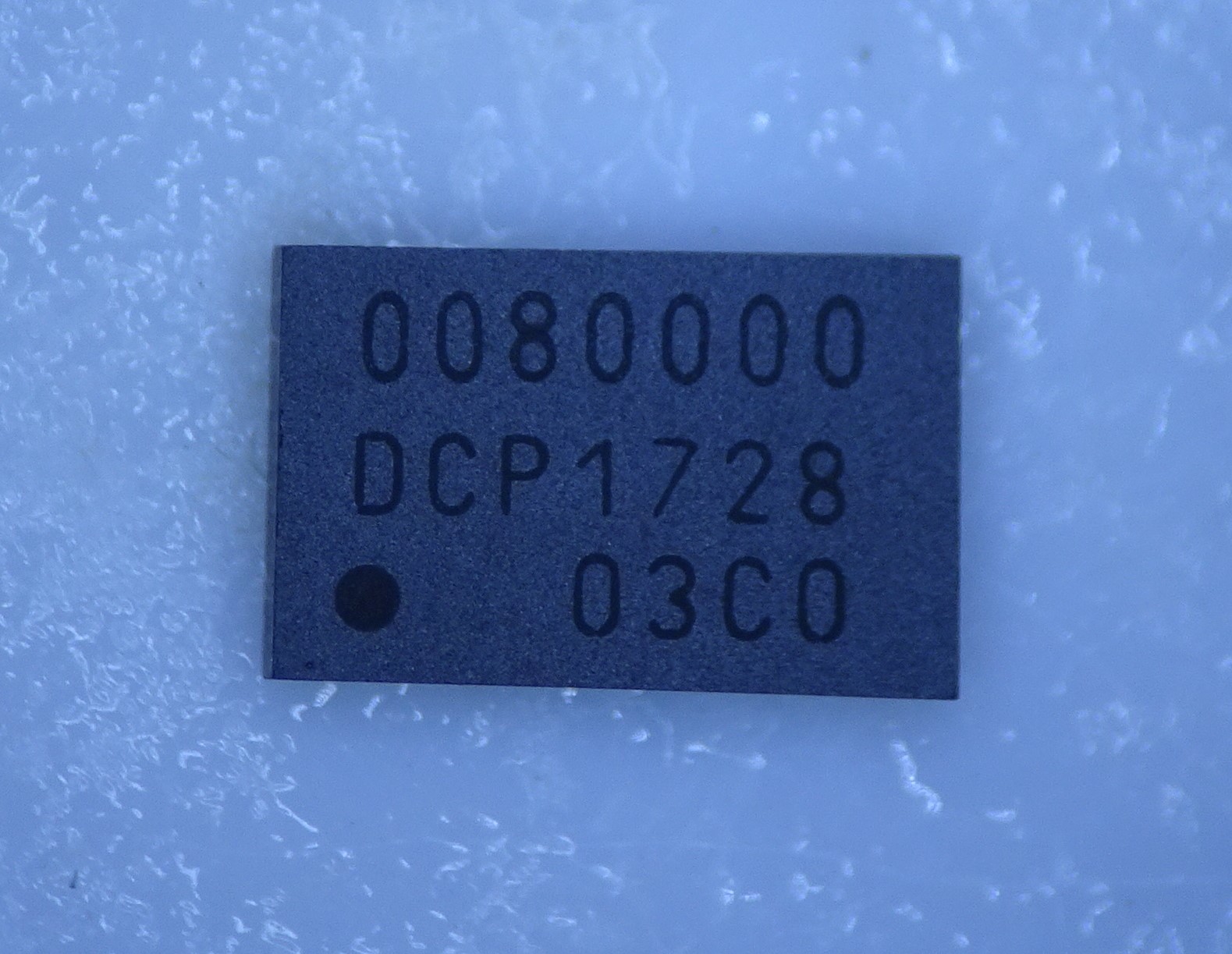
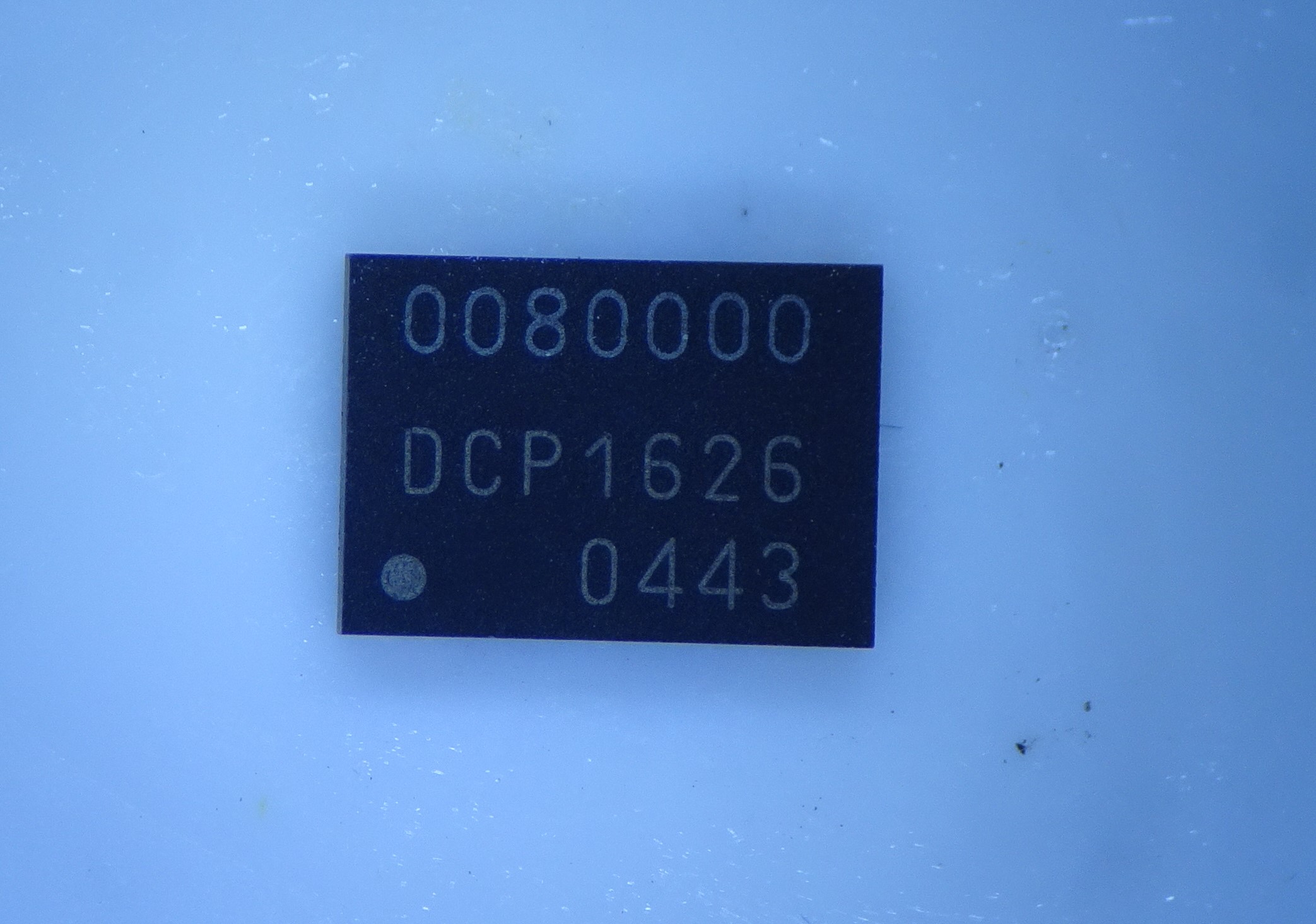
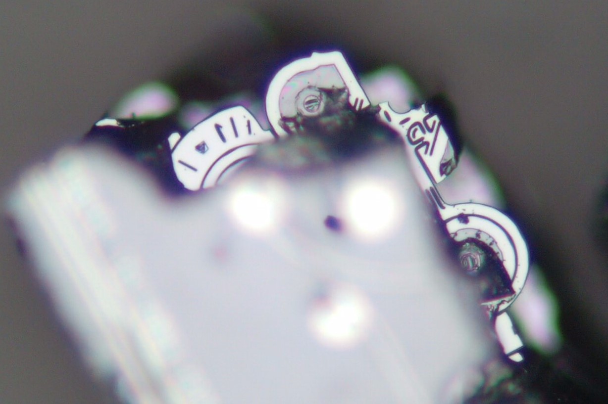
Up next is the ASFLMB sold by Abracon. The package doesn’t make this very clear, but it does include the frequency (8.0000 MHz). Abracon is an American company that mainly sells oscillators and RF products like inductors and antennas.
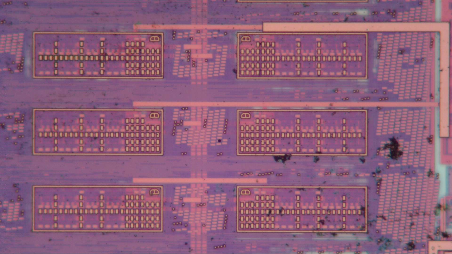
Inside, we find a two-die solution, with the control electronics on the main die and a separate MEMS die placed on top. Below is an image of the main die; the secondary die was sitting right in the middle, with bond wires running to the pads on the lower left side.
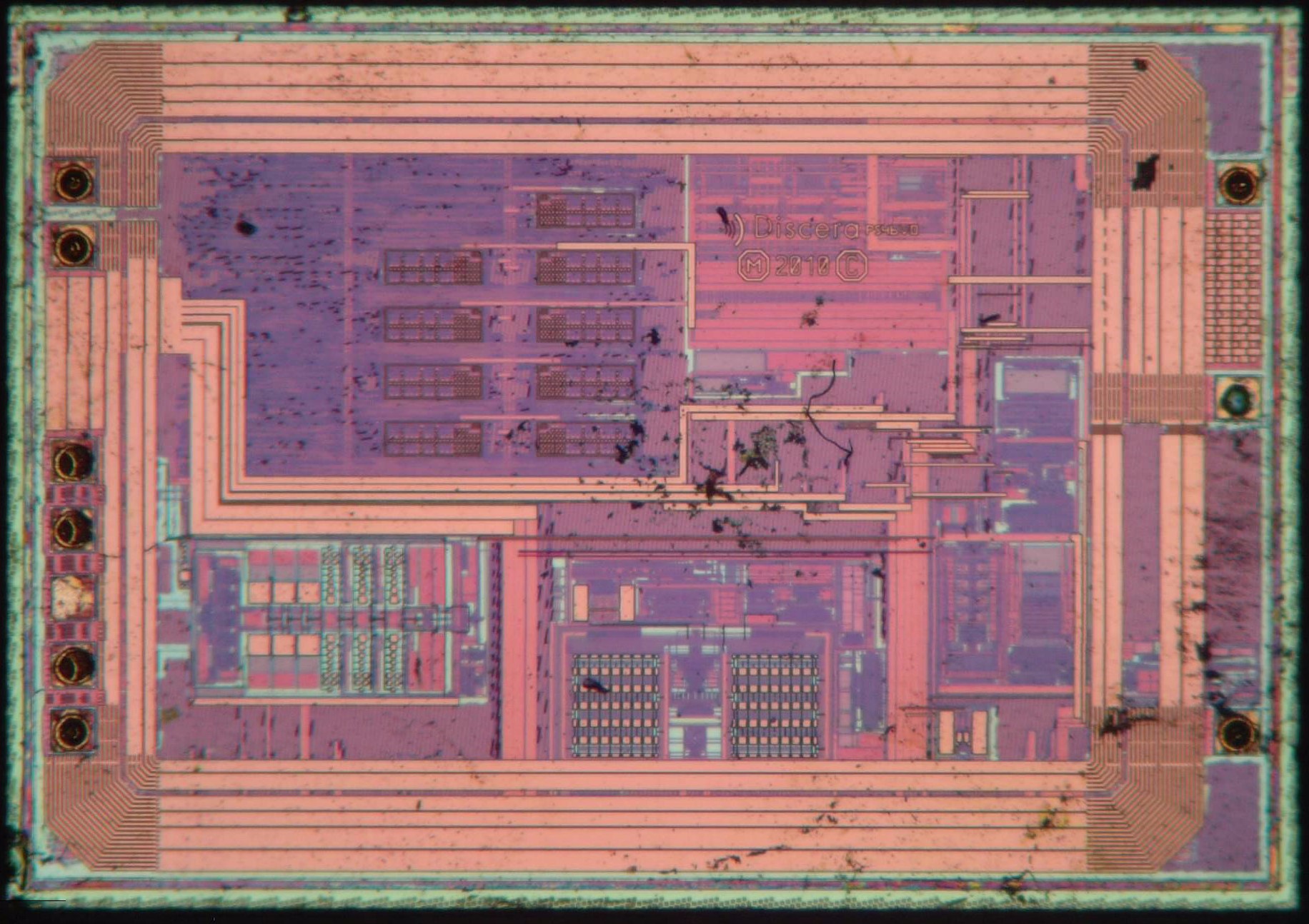
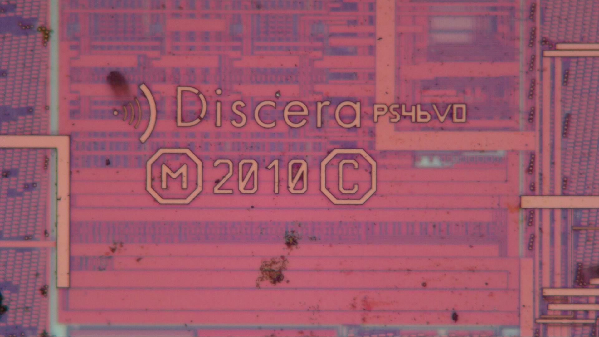
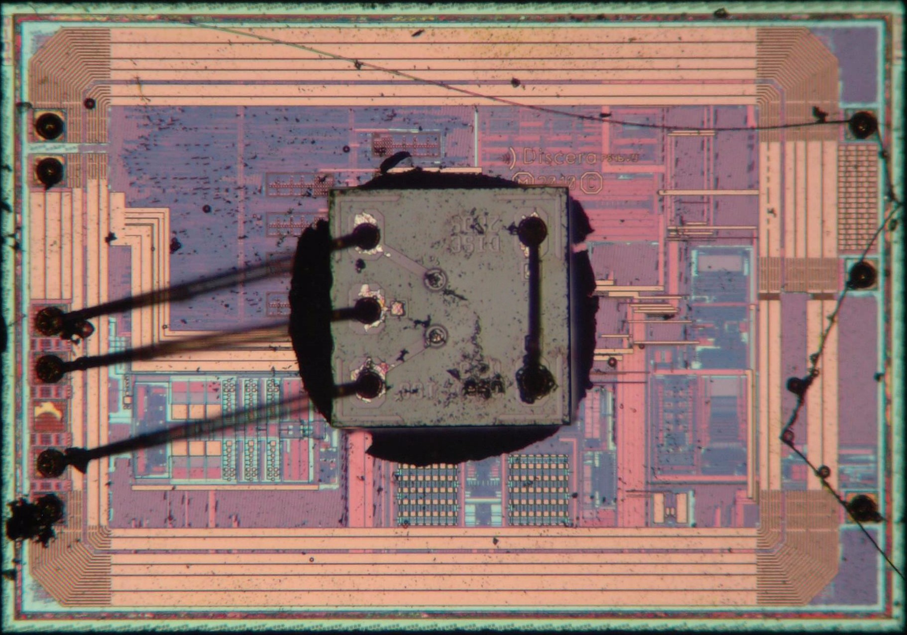
Oddly enough, the name “Abracon” is nowhere to be found. Apparently this chip was designed by Discera, a company that specialized in MEMS oscillators. The internal part number appears to be PS4bV0 (or is that a 6?). Discera doesn’t exist as a separate company any more; it was bought by Micrel in 2013, which was subsequently acquired by Microchip in 2015.
Towards the lower left corner we find this interesting-looking circuit. It looks like it has several strings of different-sized capacitors, so it might be an analog-to-digital converter of some sort.
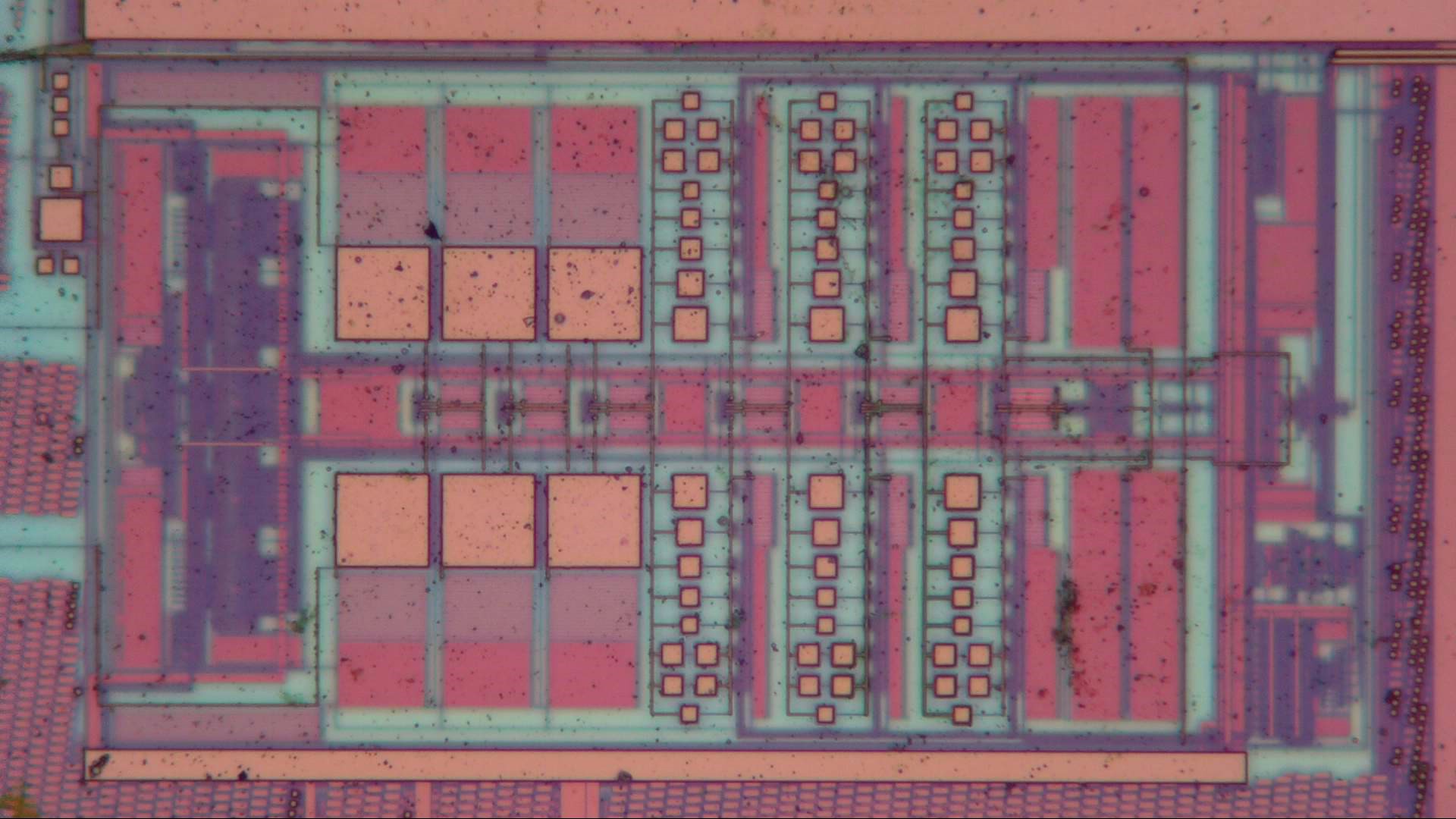
On top of the digital section are these blocks labelled “B”. It might be that these are jumpers, used to select different options in the circuitry below. That way, the manufacturer can design different versions of the same chip by changing only the metal layer in this area.
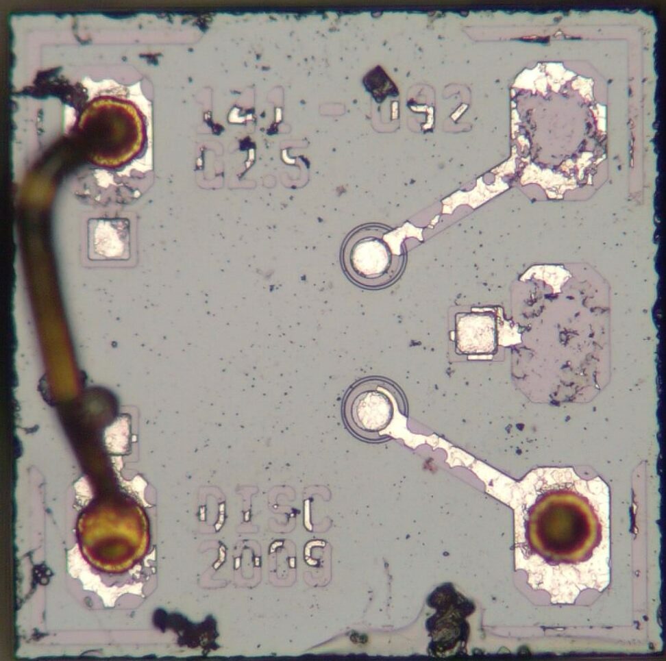
The secondary chip is made in an entirely different process. It was bonded to the primary die by the three bond pads on the right, and also has a bond wire that connects two pads together. The part number shown is 141-092 and it’s apparently a G2.5 version, designed by Discera in 2009.
A Microchip application note describes how this chip works: apparently, there are a couple of free-hanging beams inside a cavity below the surface of this chip, with through-silicon vias (the two circles) connecting to them. When a voltage is applied, the beams physically oscillate just like a quartz crystal.
It looks like the MEMS die consists of two halves that were glued together. We can just see a tiny line dividing the top and bottom halves.
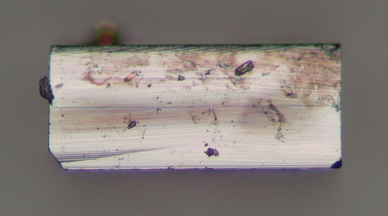
Naturally, I’d like to find out what’s inside. But cleanly separating those two halves turned out to be impossible, and in the end the only option was to use brute force. This shattered the chip into a thousand tiny shards, but luckily I was able to find some MEMS structures among the debris, as you can see below. This piece is about 100 by 200 microns, and clearly shows the same structure as seen in figure 2 of the Microchip application note. The beam in the middle is the vibrating element, supported by four anchors that hold it onto the substrate, with an electrode connected at the bottom.
Next we’ll look at the Microchip DSC1001. It looks suspiciously similar to the Abracon part, with just a slightly different part number.
Inside we find the exact same chips. It actually makes sense that Microchip uses the Discera/Micrel design, since they’re the owners of those companies now. Perhaps Abracon licensed the design from Discera at some point when it was still independent, because it would be unlikely that Microchip would design a part for their own competitor.
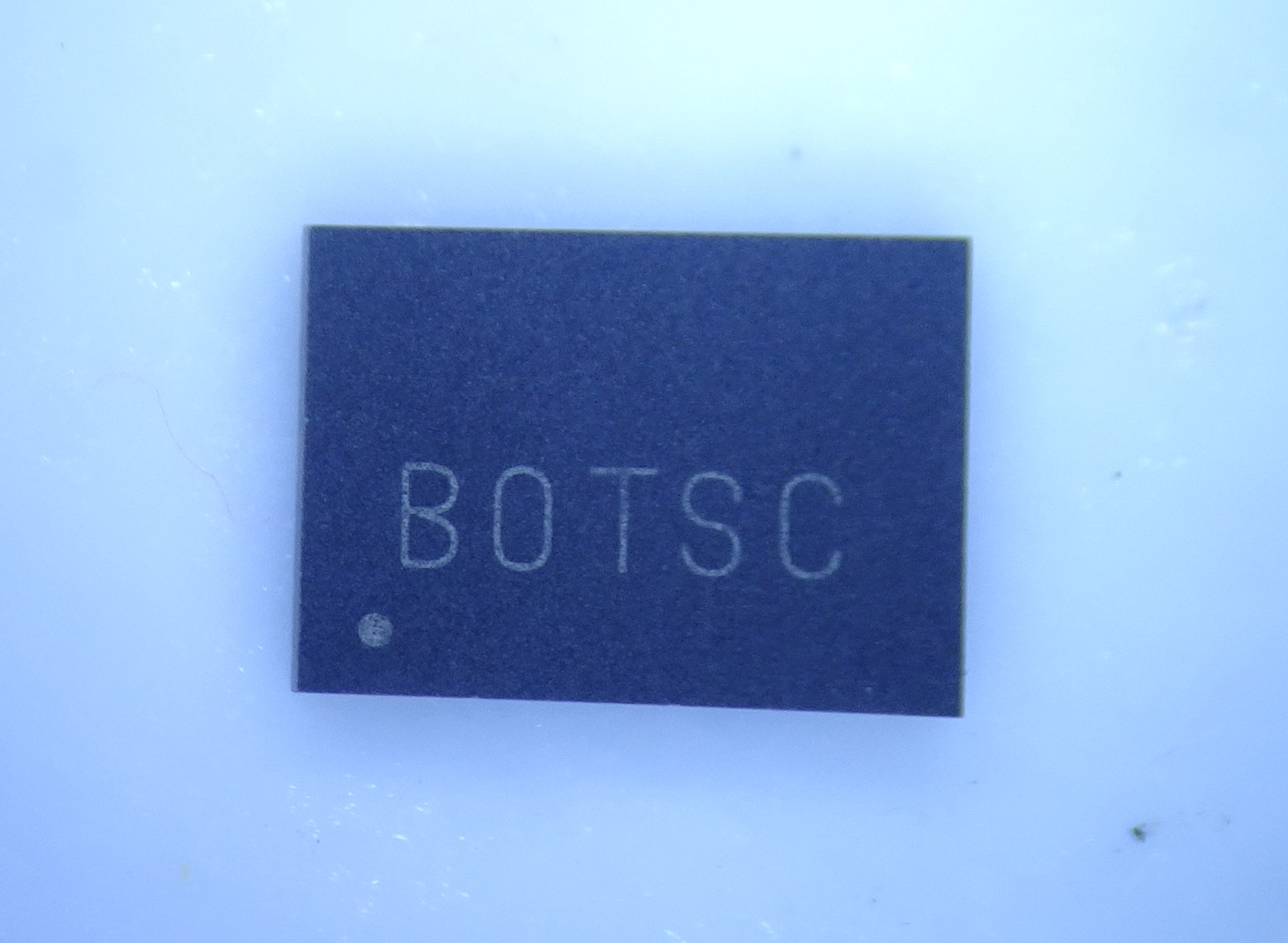
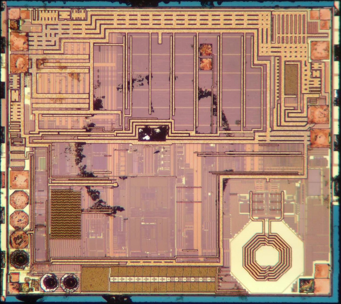
Next in line is the SiT8008B manufactured by SiTime, an American company that specializes in MEMS oscillators. The package shows just a cryptic “BOTSC”, again with no manufacturer logo or any identifying features.
SiTime also went for a two-chip solution using bond wires. Again, I had to combine two photos to get both chips in focus.
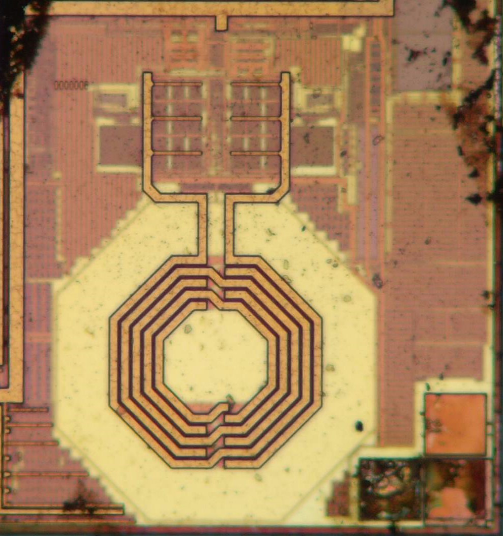
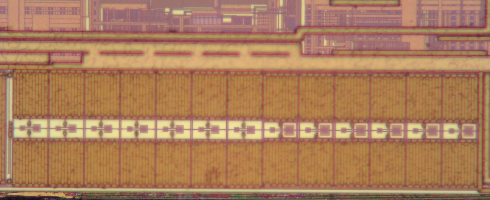
The primary die has lots of analog and digital circuitry, as well as an on-chip inductor, visible in the bottom-right corner. That’s quite unusual because inductors are typically only seen on RF chips, which this isn’t. Also interesting is the presence of what looks like two bond pads in the middle of the chip: these might be used to connect to the substrate of the secondary die.
Zooming in on the inductor we see that it’s a single wire making six turns using two metal layers. On-chip inductors are typically only useful at frequencies in the GHz range, so I’m a bit puzzled to see it in this 8 MHz oscillator.
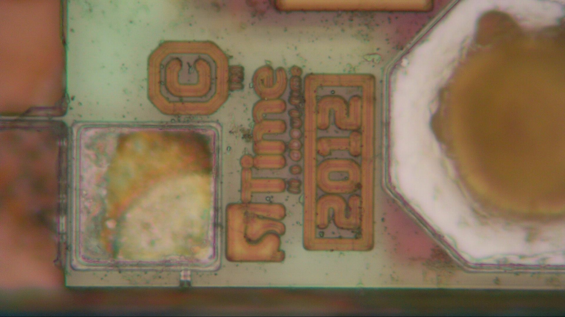
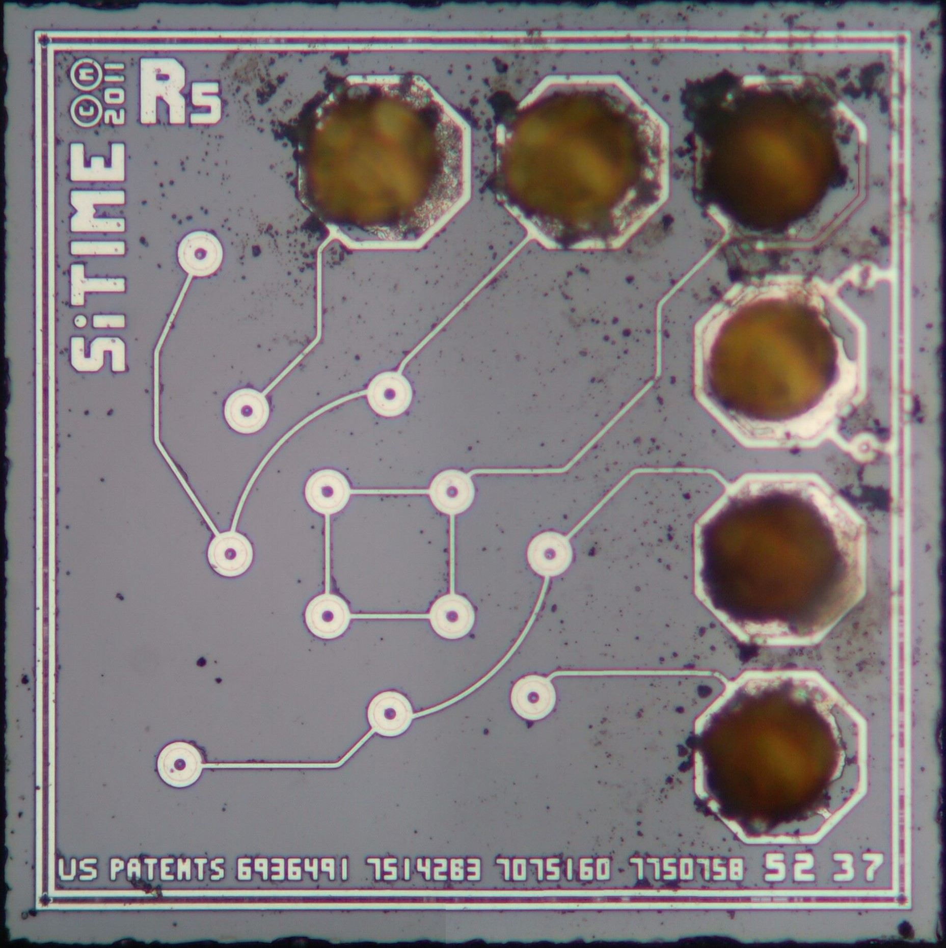
The main die shows a 2012 copyright date, next to the SiTime logo. Also, just about readable, is their slogan, “It’s about time”. Clever!
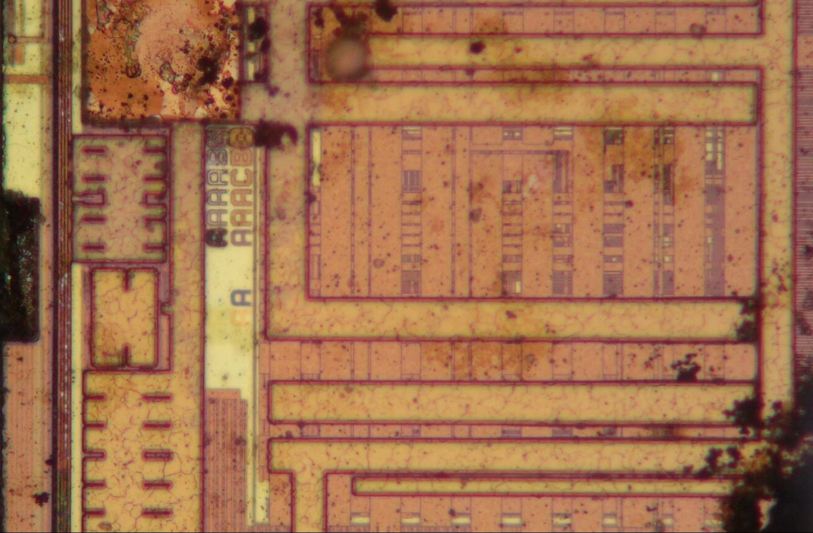
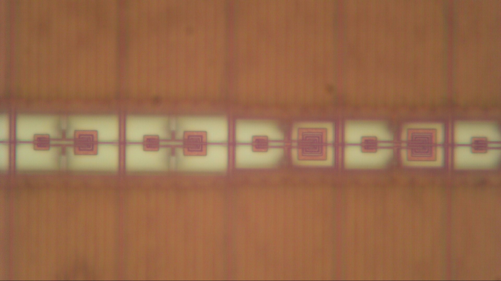
Many of the circuits, especially in the digital section, are obscured by lots of metal. We can see a set of revision letters though: most are “A”, but there are a few “B”s and even the occasional “C”.
Towards the bottom of the die we find this interesting circuit that consists of two slightly different halves. This could be part of an analog-to-digital converter (as we saw on the Abracon and Maxim parts), or perhaps of some frequency-adjustment circuit.
Zooming in on those small features in the middle, we find that they look transistors in two different sizes.
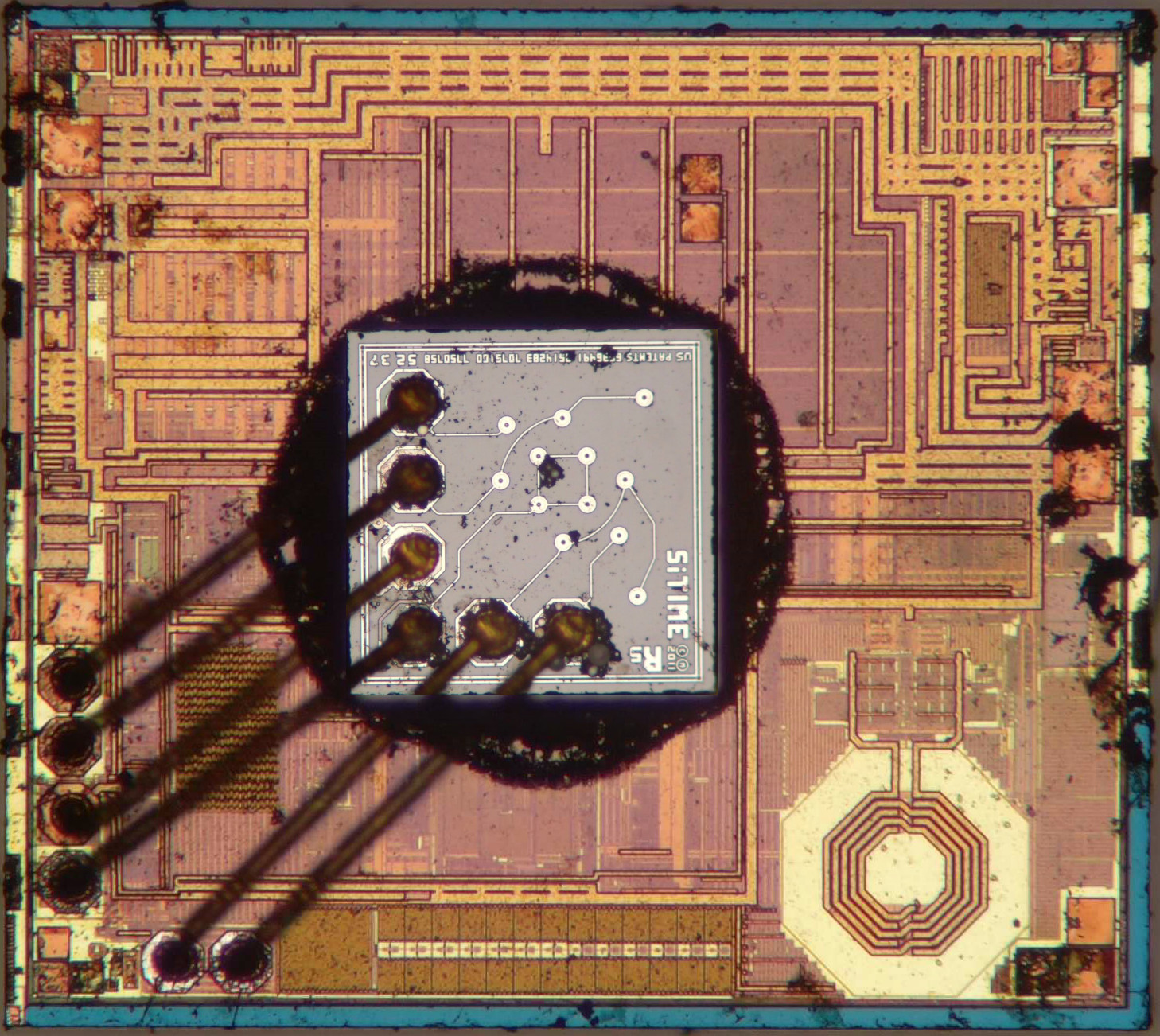
The MEMS die is bonded to the main chip through six bond wires. It has a 2011 copyright date and helpfully shows a few patent numbers that are relevant to its design: US6936491, US7514283, US7075160 and US7750758. These describe a way of encapsulating silicon microstructures in a hermetically sealed enclosure, similar to the system used by Discera. The real MEMS bits are hidden below the surface, with connections to the outside world formed by through-silicon vias.
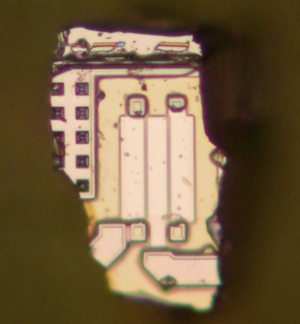
SiTime’s MEMS die similary consists of two halves bonded together.
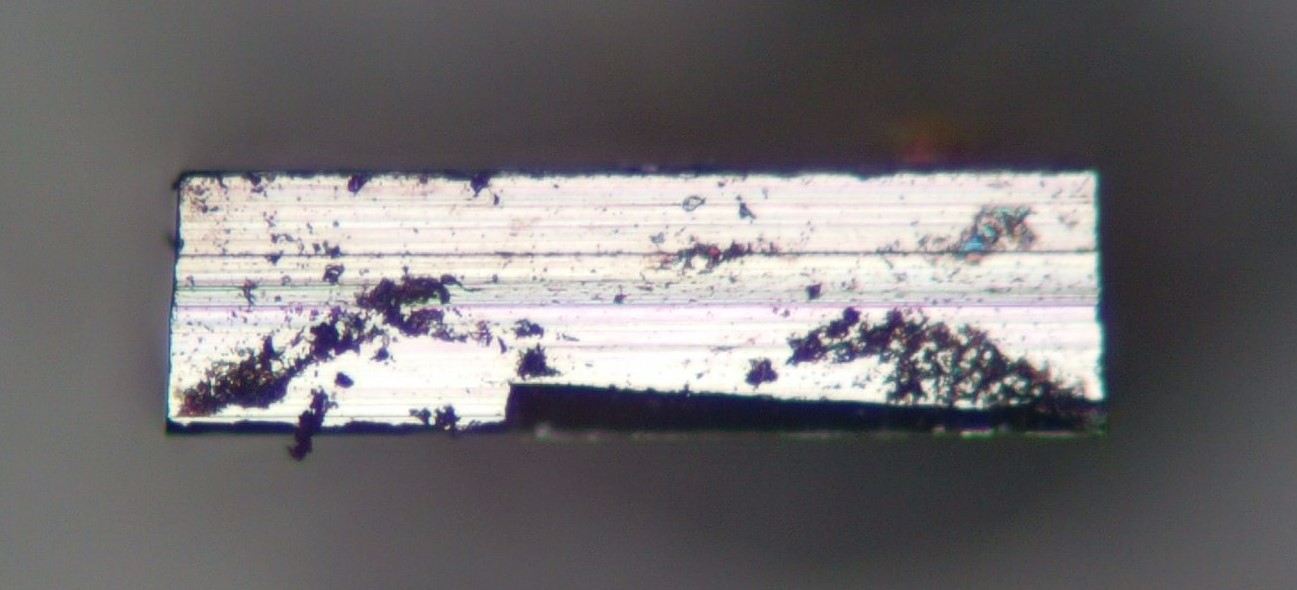
This time I was a bit less lucky when I tried to open it up: most of what I was left with was just silicon powder. The only recognizable bit was this section, where we can clearly see one corner of what used to be the resonator. It’s mounted through a flexible piece, somewhat similar to what we saw in the Abracon part.
MEMS chips are typically very interesting to look at, but difficult to disassemble. I’ll see if I can come up with a less destructive way of opening silicon dies – maybe there’s some etching or polishing method that I can use.