Although the 555 timer is one of the most iconic chips ever made, and the original version is still sold in huge numbers, it actually makes little sense nowadays to use the classic chip anymore. That’s because an improved version has been around for a long time: the CMOS 555 timer. Most manufacturers that produced the original bipolar 555 timer also make a CMOS version, with typically the letter “C” somewhere in the full product name. Today we’ll have a look at a couple of these CMOS timers and see how they differ from the bipolar model.
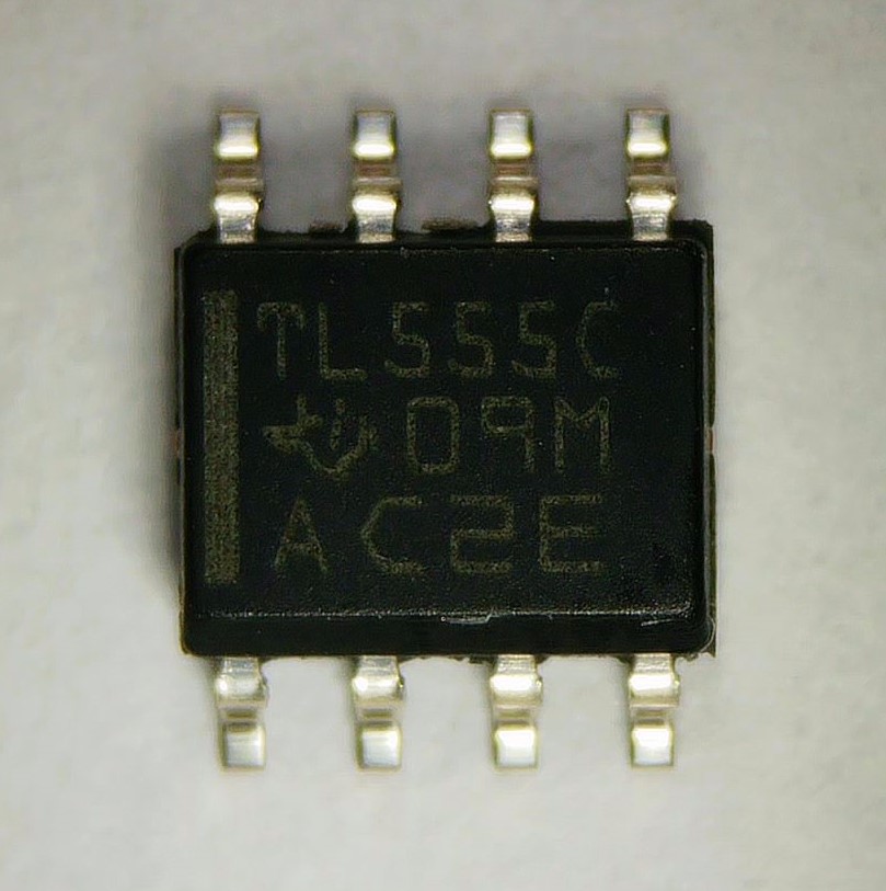
First up is TI’s TLC555. The pinout and functionality are exactly the same as the original chip’s, but the electrical specifications are a bit different, especially when it comes to power consumption: where the classic 555 uses up to 15 mA from a 15 V supply, the CMOS version uses just 600 uA. It can also run at higher frequencies, up to 2.1 MHz, where the bipolar version struggles to reach much more than 100 kHz. The only drawback of the CMOS version is its limited output current: it can sink up to 100 mA and source just 10 mA, instead of the symmetrical 200 mA that the classic 555 can deliver.
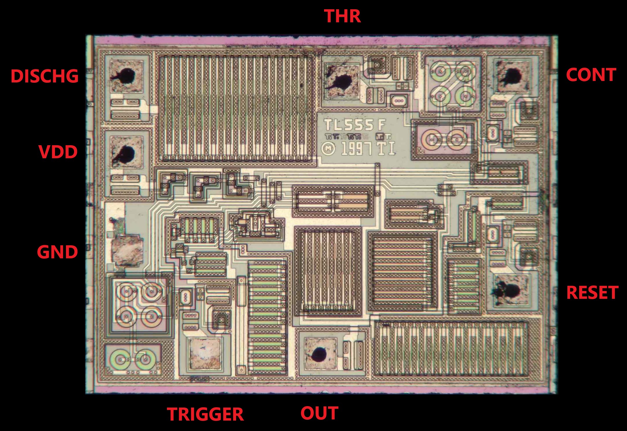
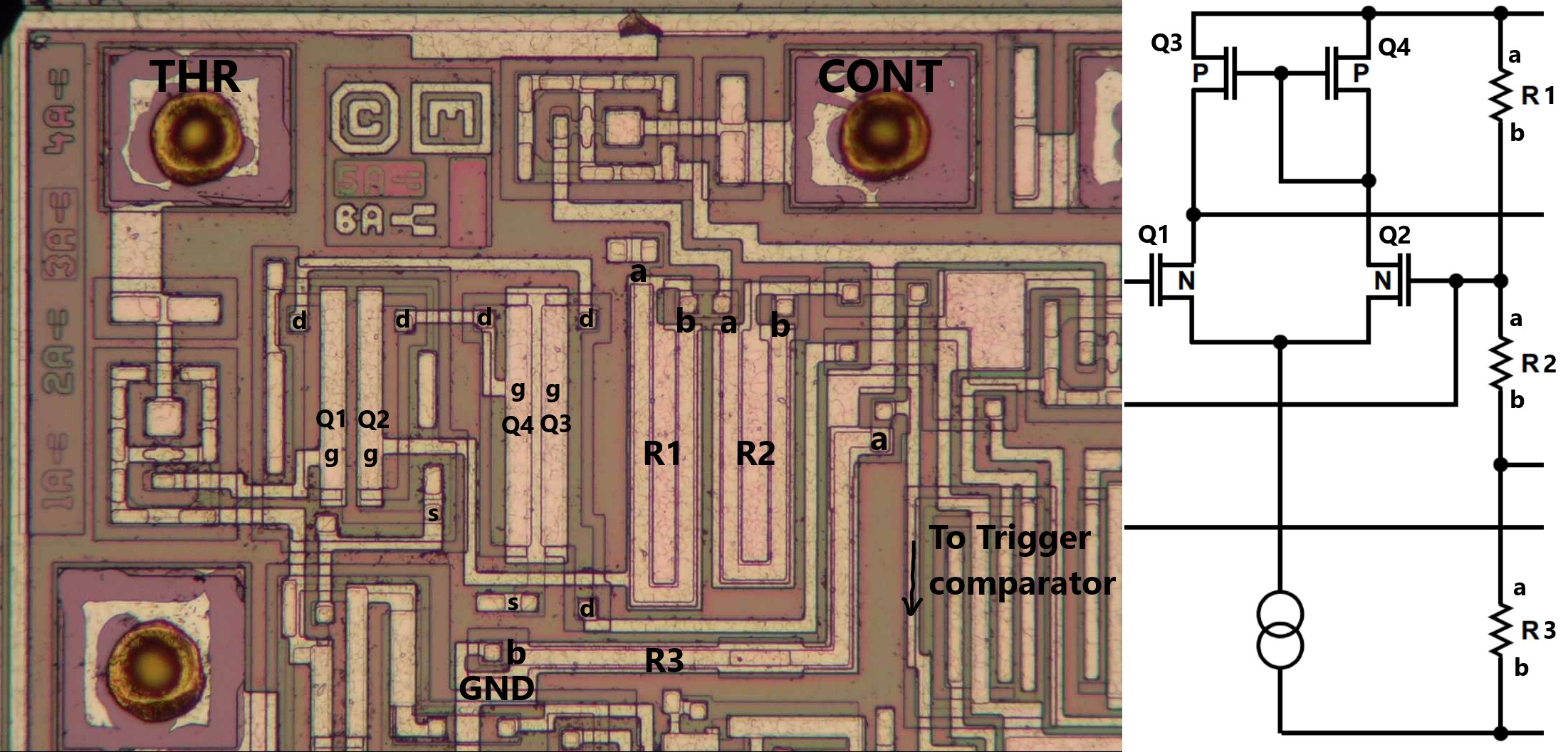
Inside we find this pretty design. From the larger transistors you can clearly tell that this is a CMOS design: large MOSFETs are typically made from a set of “fingers” in parallel. What is quite unusual is the presence of round transistors in the top-right and bottom-left corners. These are the trigger and threshold comparators, so my first guess is that round transistors might have better matching performance.
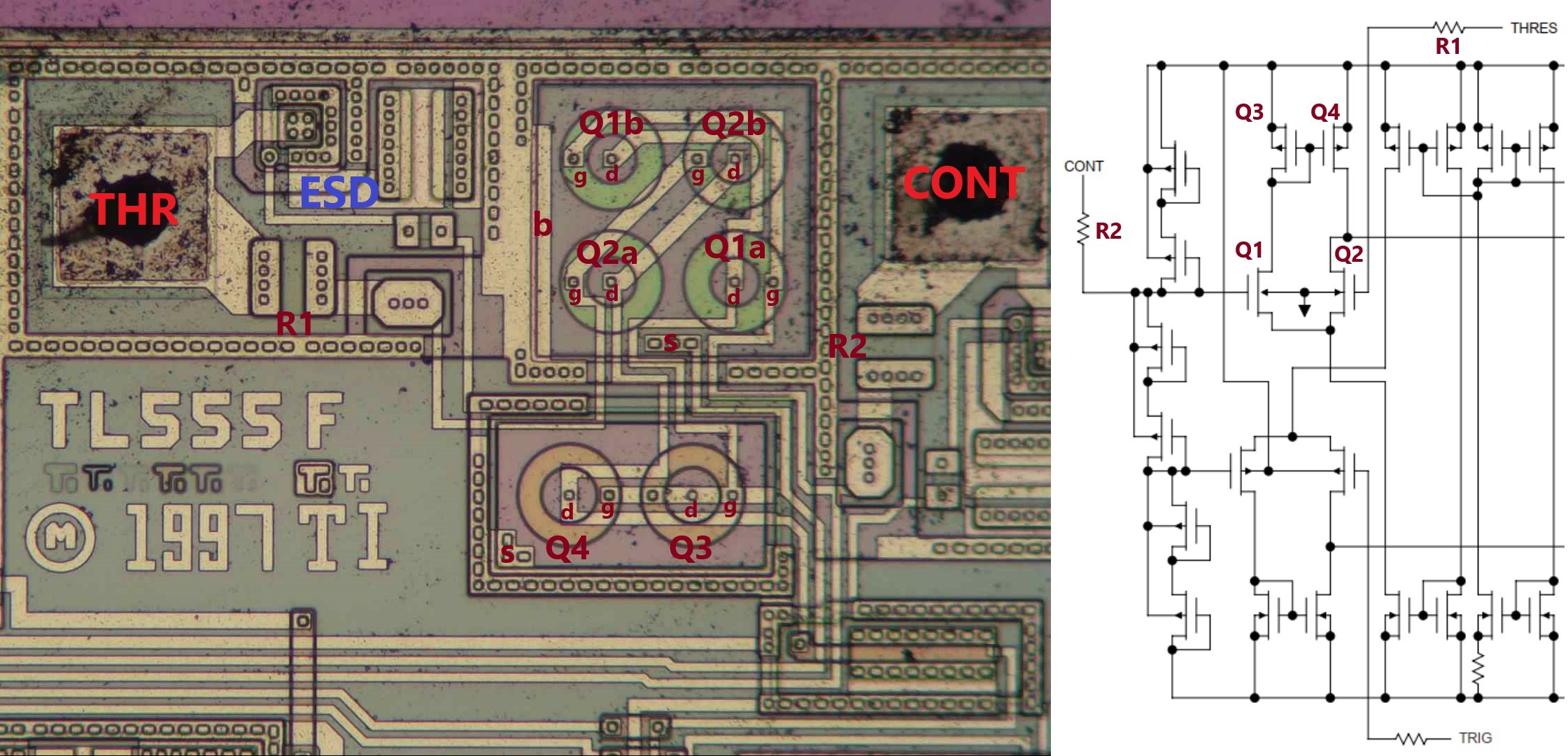
If we follow the wiring around the threshold comparator, and compare it with the schematic as shown in the datasheet, we find several interesting things. First, the NMOS differential pair Q1/Q2 is laid out as a cross-coupled pair. That is, Q1 and Q2 are both split into two identical, parallel transistors, which are then placed in a square. This helps to improve the matching of those two transistors, and thereby reduce the input offset voltage. Since Q1 and Q2 share a source terminal, this is brought out using a single contact at the bottom. They also share a bulk (or body) contact, connected to GND.
The ESD structures are more complex than the single resistor shown in the schematic. It looks like there are bipolar clamps and secondary diodes as well. CMOS transistors are far more susceptible to ESD damage, so it makes sense that there’s more protection circuitry here than there was in the bipolar version.
This layout has a 1997 copyright date, and layer markers made from little “Ti” logos. That’s a nice touch, because usually these markers are just boring As or Bs.
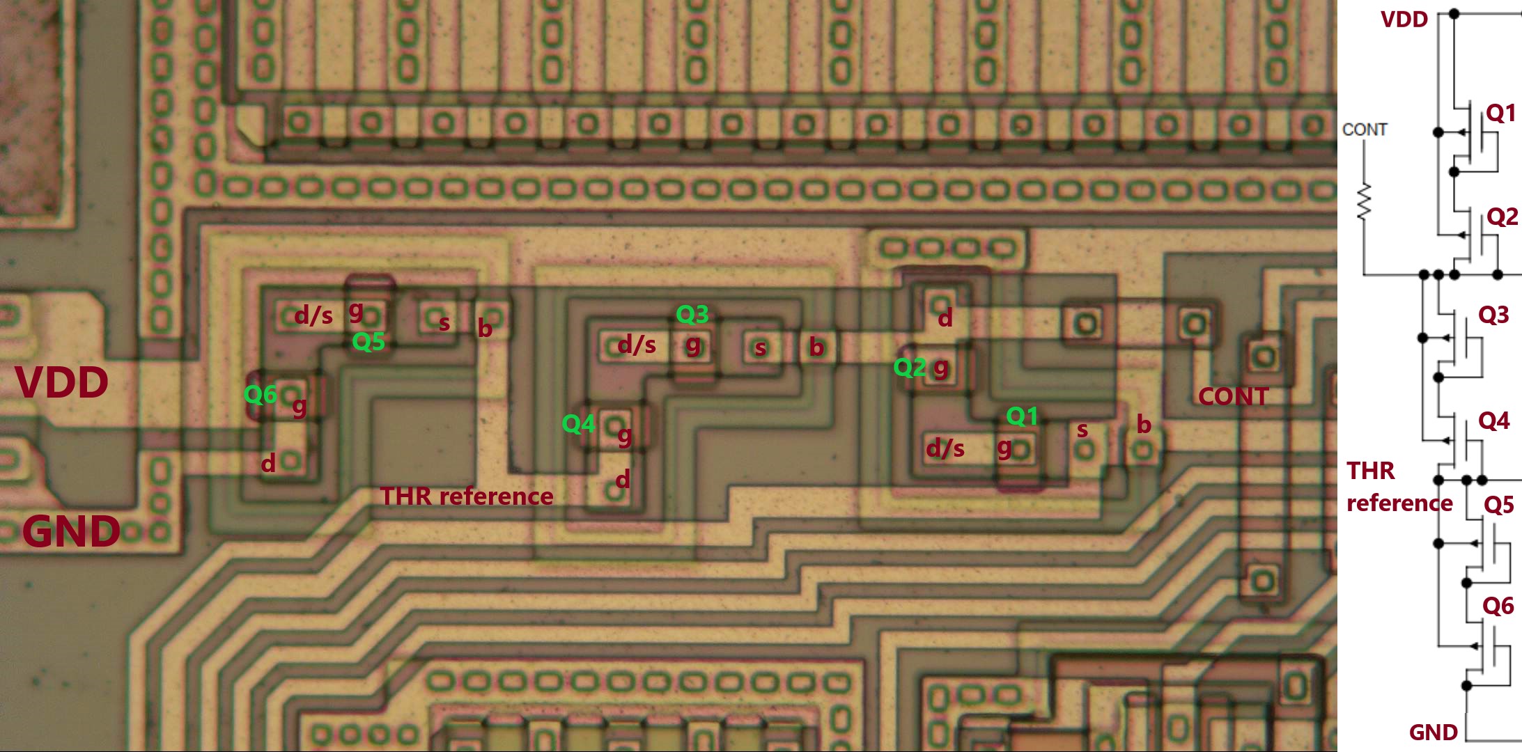
The reference generator circuit is also interesting to look at. Where the bipolar version comes with three long, 5 kΩ resistors, the CMOS version has six diode-connected PMOS transistors. Q1 and Q2 have their body connected to VDD, and share a single contact for Q1’s drain and Q2’s source. Q3 and Q4 share a body connection to CONT, while Q5 and Q6 are connected to the THR reference. Each pair of transistors acts as a resistor of about 80 kΩ, for a total resistance of 240 kΩ.
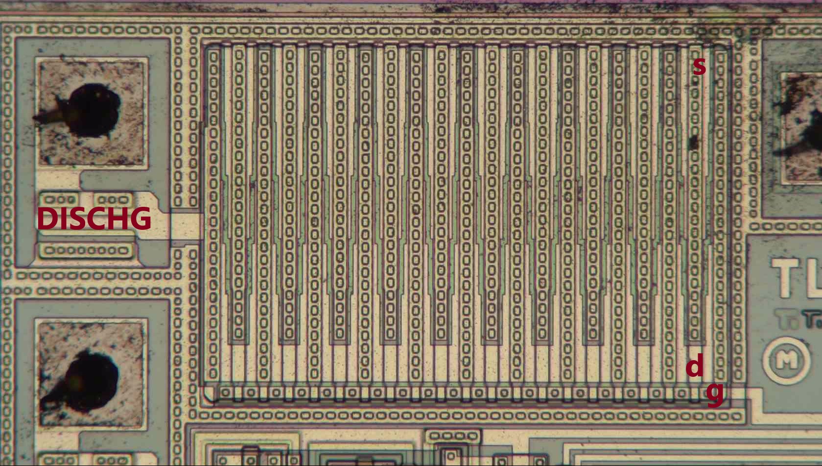
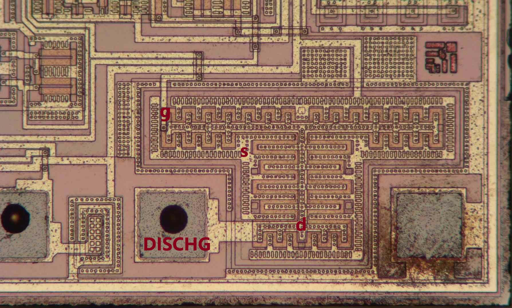
The discharge transistor is a typical example of an MOS power transistor. It’s divided into a large number of fingers, each of which carries one portion of the total output current. The gate connection, at the bottom, is connected to long vertical strips of polysilicon, which is the space between the source and drain terminals. Current then flows horizontally from drain to source.
Note how the metal on top of the source and drain terminals starts out wide and gets progressively thinner along the finger. This is designed that way because the current is largest at the beginning of the finger and gets lower towards the end.
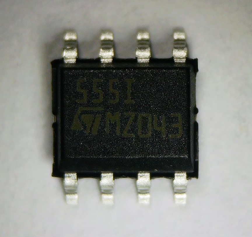
Next up is the TS555 made by STMicroelectronics. The package has a rough surface with laser markings that are very hard to photograph.
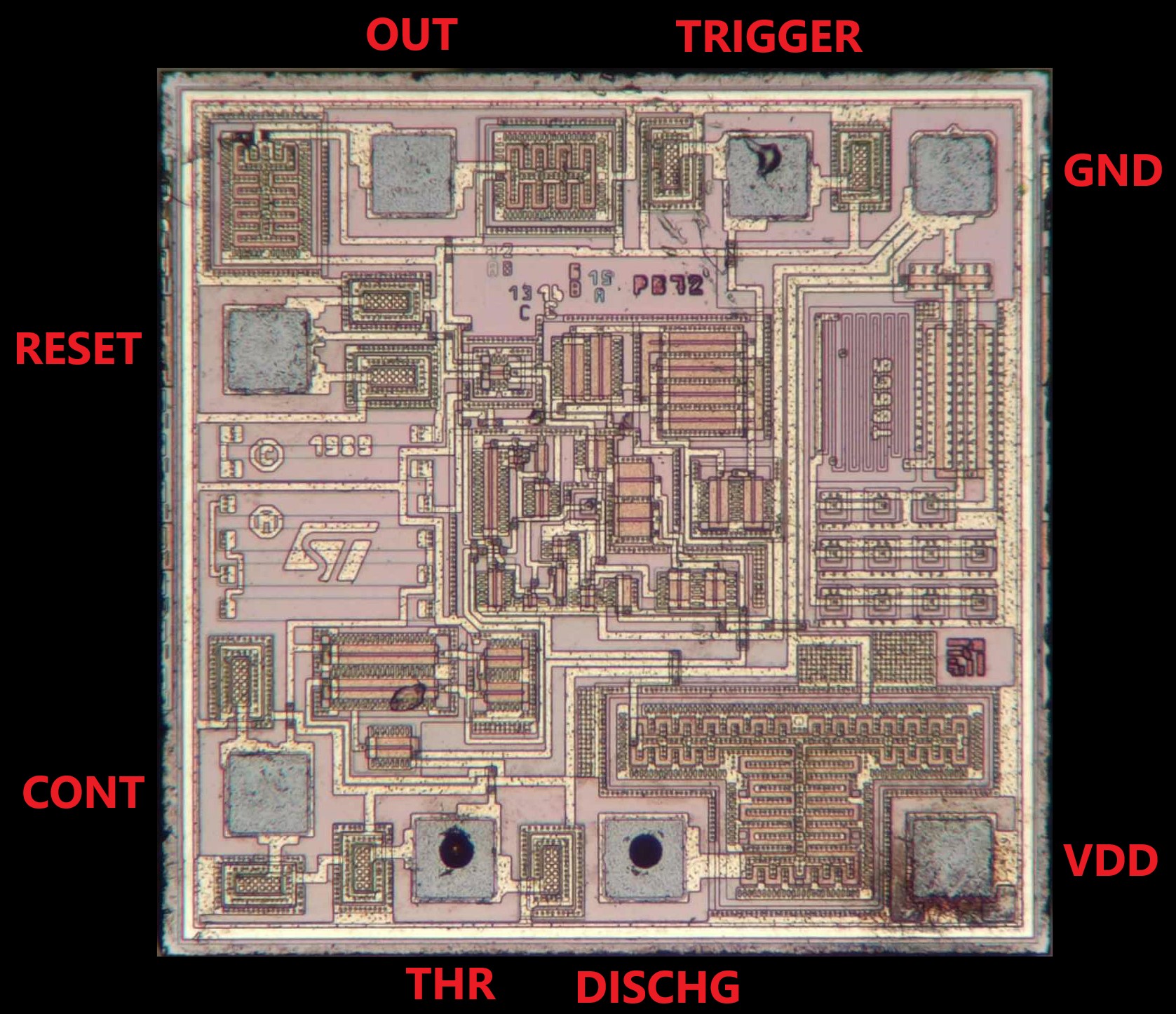
The insides look completely different to TI’s. First of all, we notice that the power transistors near OUT and DISCHG have a serpentine layout instead of TI’s finger layout. There are also long resistors, one set below the ST logo on the left and a long, thin one on the upper right side. Finally, there seems to be a set of bipolar transistors in the middle-right section.
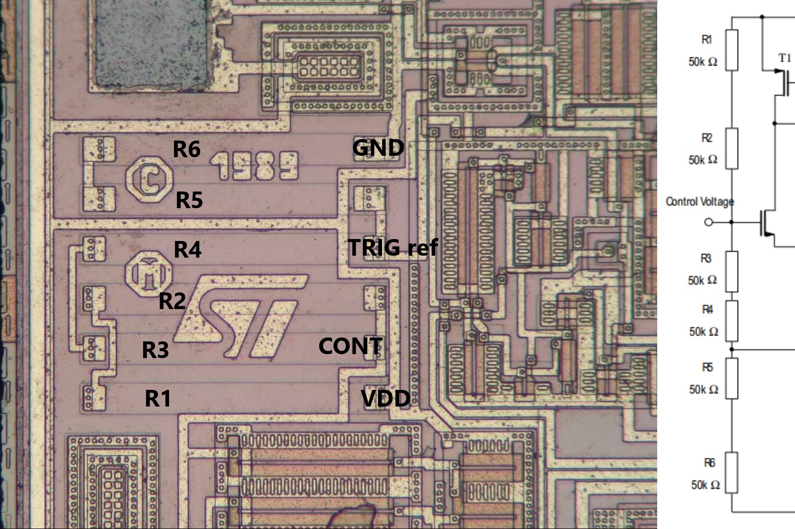
Here we see the resistors that generate the reference levels. The designers at ST decided to use polysilicon resistors, and chose to interdigitate two of them (R1/R2 and R3/R4). This improves the matching of those two resistors, but leaves R5/R6 out of it. It’s not really possible to make a good interdigitated layout of three resistor pairs, so that’s why only one pair was laid out like this.
In any case, the resistors’ matching won’t be that great, since they all have different metal shapes on top of them. This causes local deformation in the resistor layer, leading to slight differences in resistance between the six resistors. On really well-matched resistor arrays you’ll see that the designers take care to ensure that there either isn’t any metal crossing the resistors, or if there is, that it’s identical on every device.
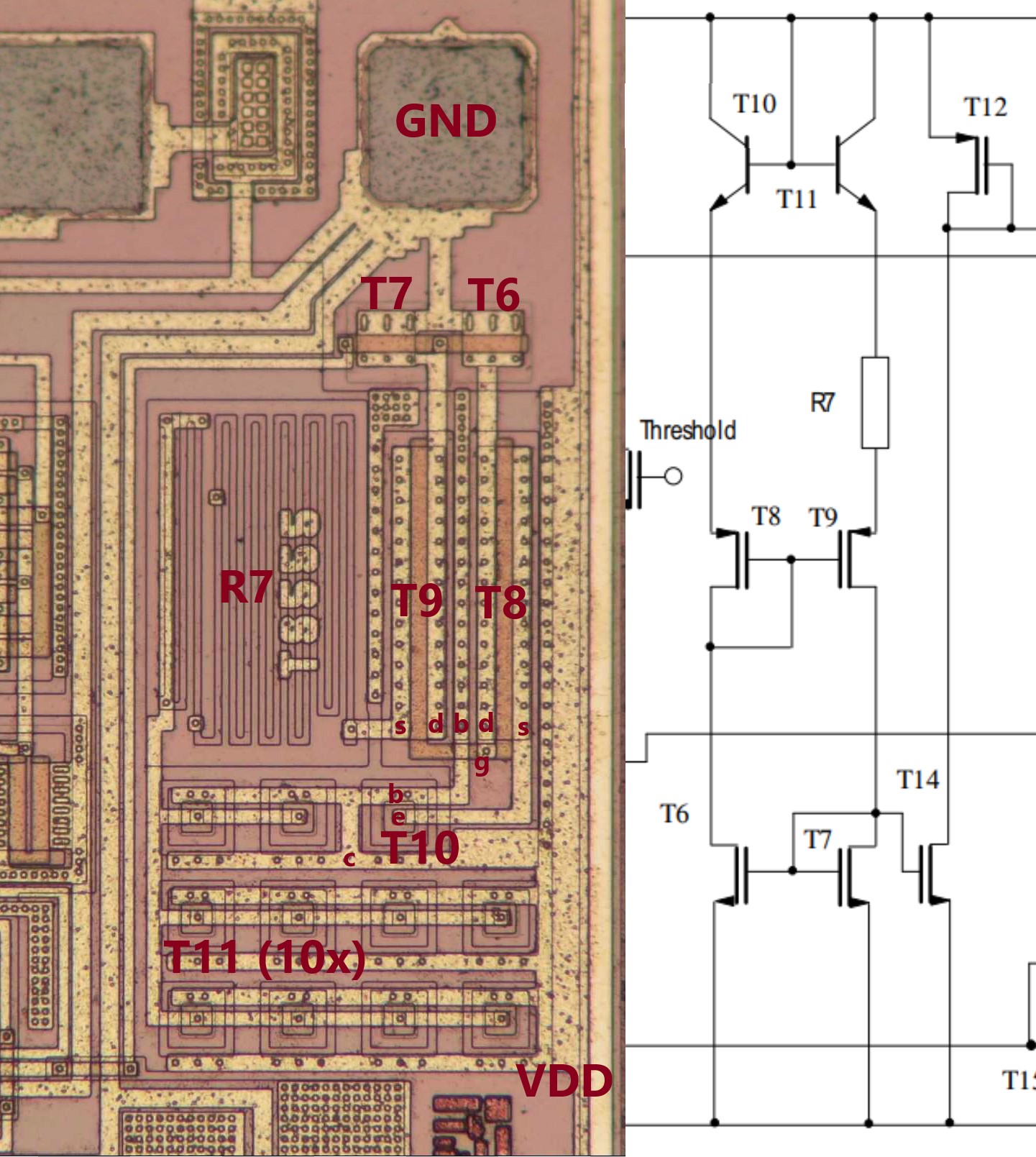
The bias current generator uses a set of bipolar transistors. The circuit that they make is a classic PTAT reference, which makes a current that is Proportional To Absolute Temperature. The reason for this is that a transistor’s transconductance, often called gm, drops with increasing temperature. By biasing everything with a PTAT current this effect is cancelled, making the total circuit perform much more consistently across temperature.
The basic idea of this circuit is as follows: T6 and T7 form a matched pair, along with T8 and T9, and since each pair forms a current mirror (gate connected to one of the drains), the currents in both branches are identical. That means the currents in diode-connected NPNs T10 and T11 are also equal. However, since T11 is ten times larger than T10 its base-emitter voltage is lower by a well-defined amount, determined by physical constants. That voltage difference appears across R7, and determines the current in both branches. T14 (which is located elsewhere) carries a copy of that current to bias other circuits.
Note how R7 has two additional vias along its path. These were placed there to allow a bit of fine-tuning of the final resistor value in production, requiring only a small change in the metal layer.
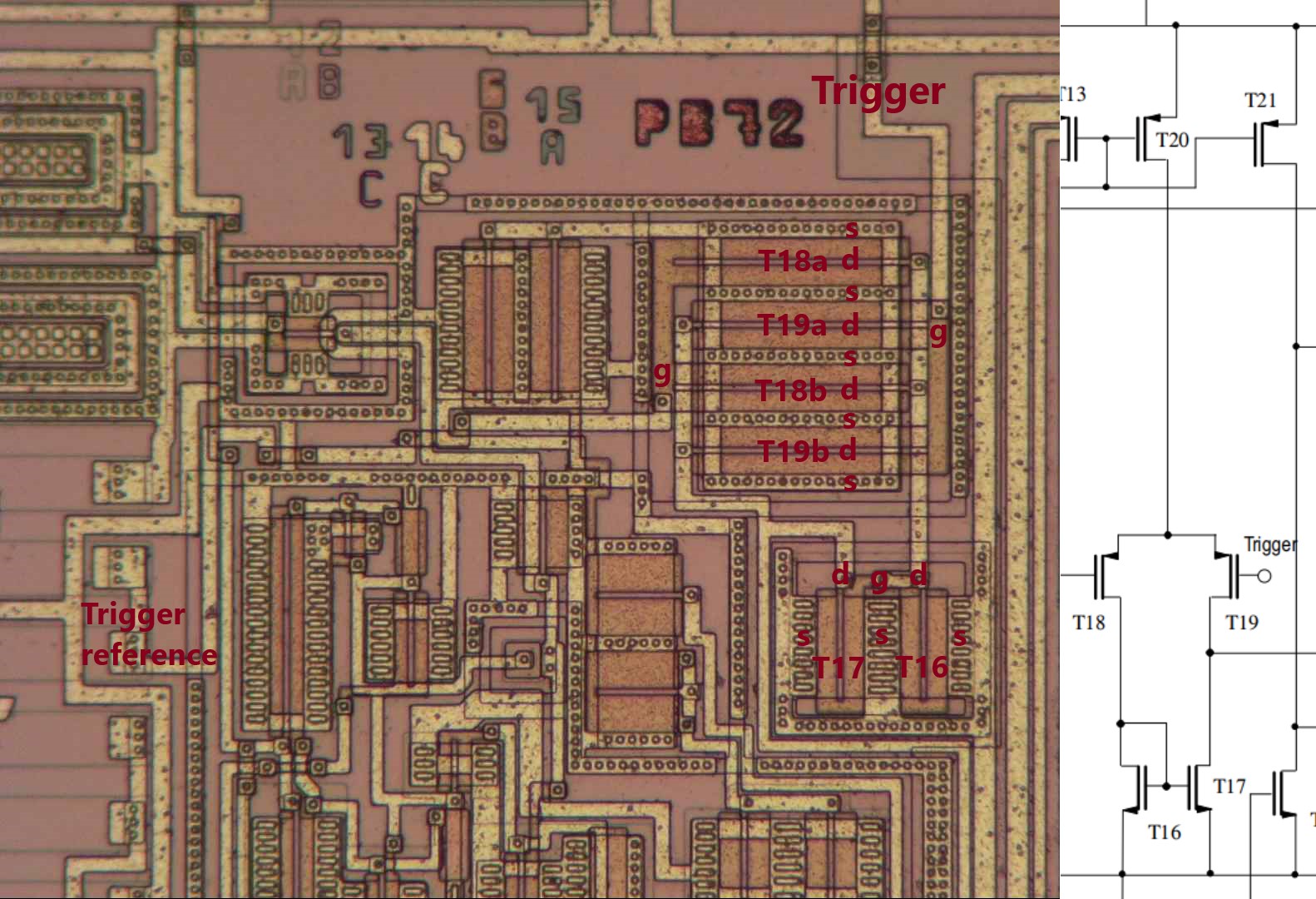
Here we can see the trigger comparator. Like in TI’s design, T18 and T19 are split in two and interleaved with each other, although the transistors are regular square ones this time, laid out in a straight line. Whether ST’s layout is optimal is debatable, however. Typically, the aim of a good layout is to ensure that both transistors have a common centroid: the “average location” of each should be at the same point for both. In this case, the midpoint of T18 is located where T19a is. Similarly, the midpoint of T19 is at T18b’s location. One could argue that it would have been better to have T18a and T18b at the top and bottom position, with T19a and T19b in the middle. Then again, transistors sitting on the outside of a row (as T18 would be in that case) also get slight deviations due to edge effects, which might cancel any benefit from having common centroids.
We also see the layer and revision designators at the top of this picture: two As, two Bs and two Cs. “PB72” must be some internal part number.
The layout style for power transistors is a bit different, too. It’s still a fingered layout, but with all drain fingers at the middle, source fingers on the outside and the gate snaking between them.
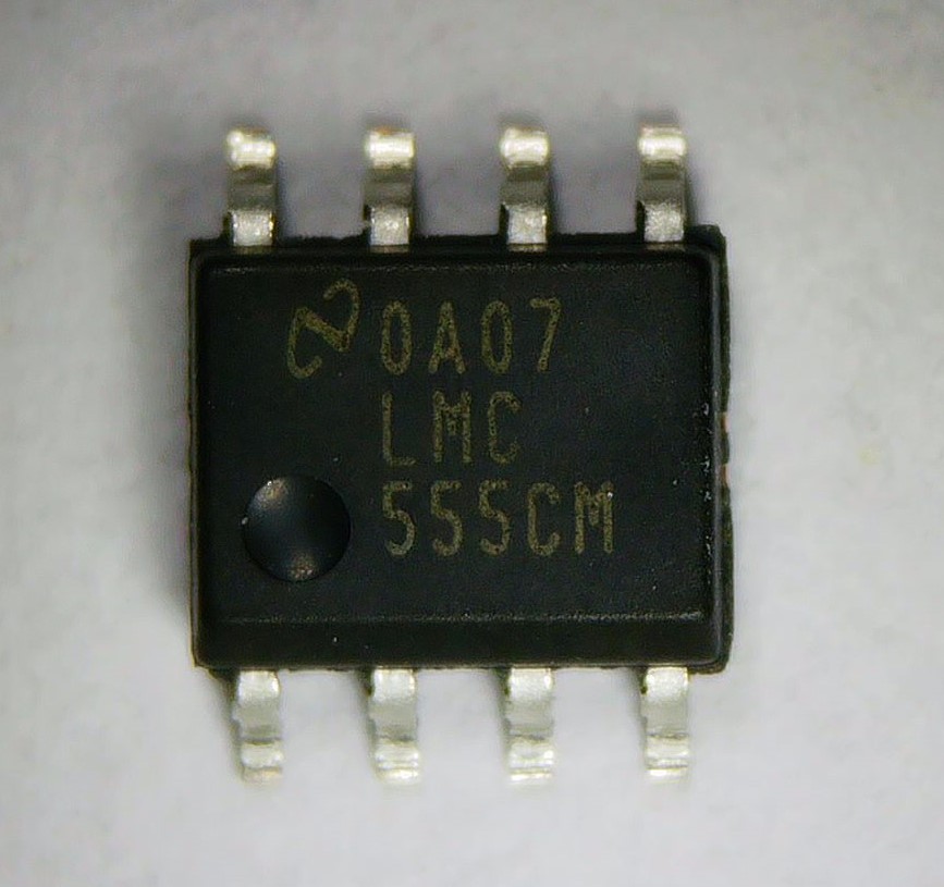
National Semiconductor also made a CMOS version of their LM555, appropriately called LMC555. Here I’ve got one in a DIP package. TI still sells this part alongside their own TLC555, just as they do with the bipolar 555 and the 741 op amp.
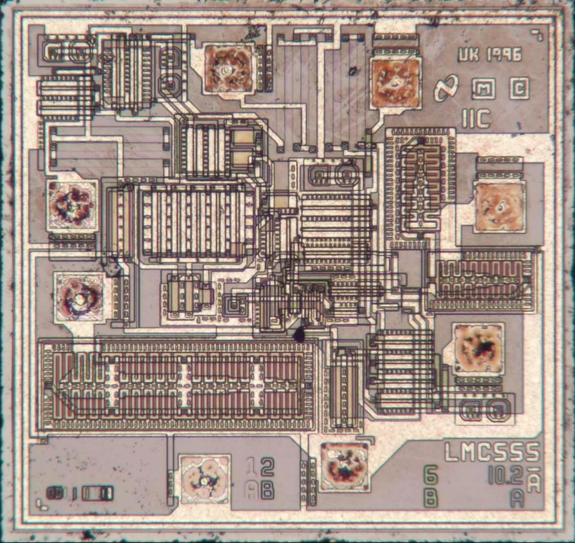
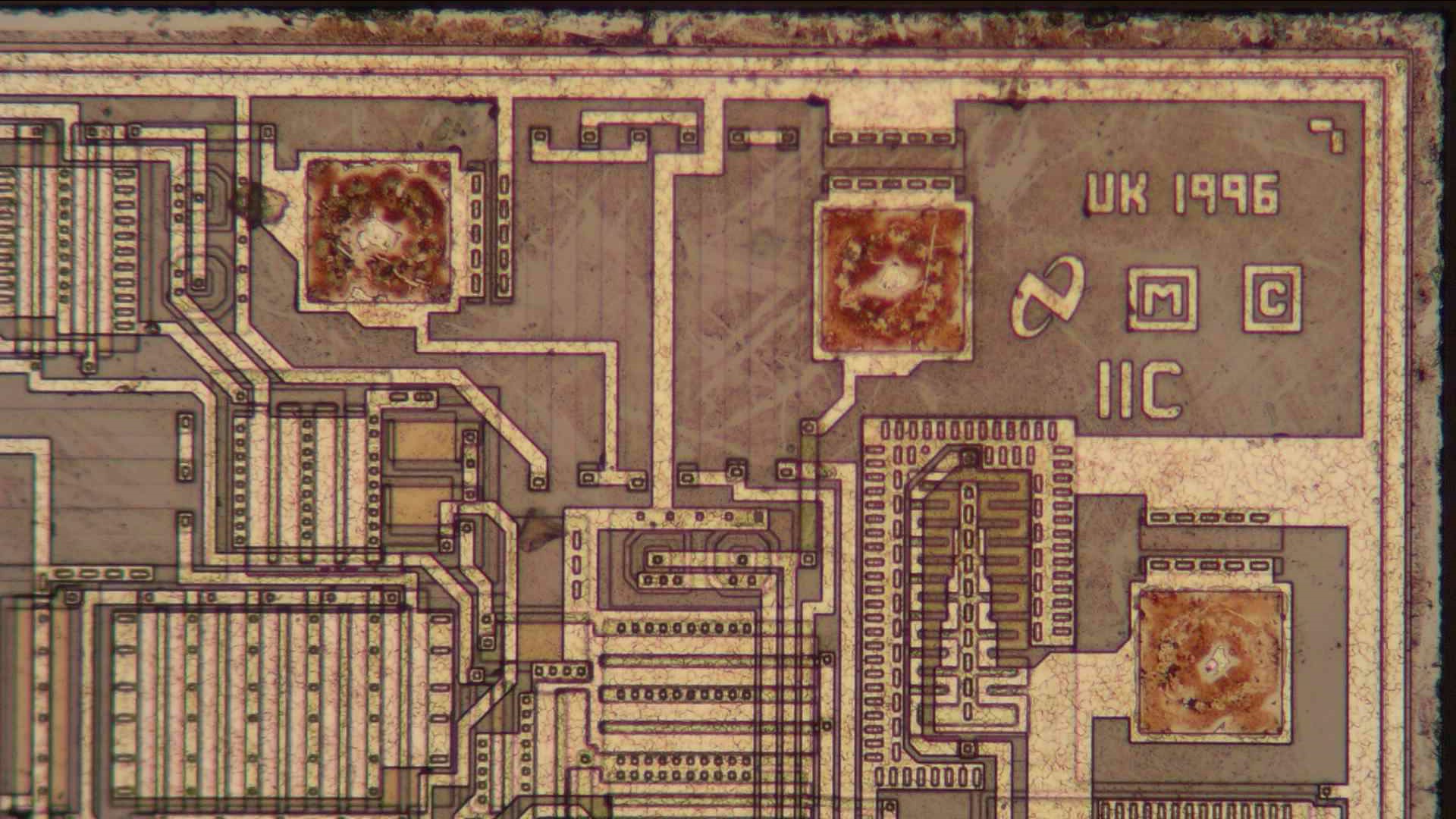
The inside looks typical. There’s quite a bit of empty space on the lower edge and in the top-right corner. There’s a 1996 copyright date as well as “UK-F3” in the bottom-left corner, which might refer to National’s UK fab in Greenock. TI inherited that fab when it acquired National back in 2012, and kept operating it until 2019, when it was acquired by Diodes Inc.
National never included an internal schematic in its LMC555 datasheet, so I went ahead and reverse-engineered the layout to end up with the following:
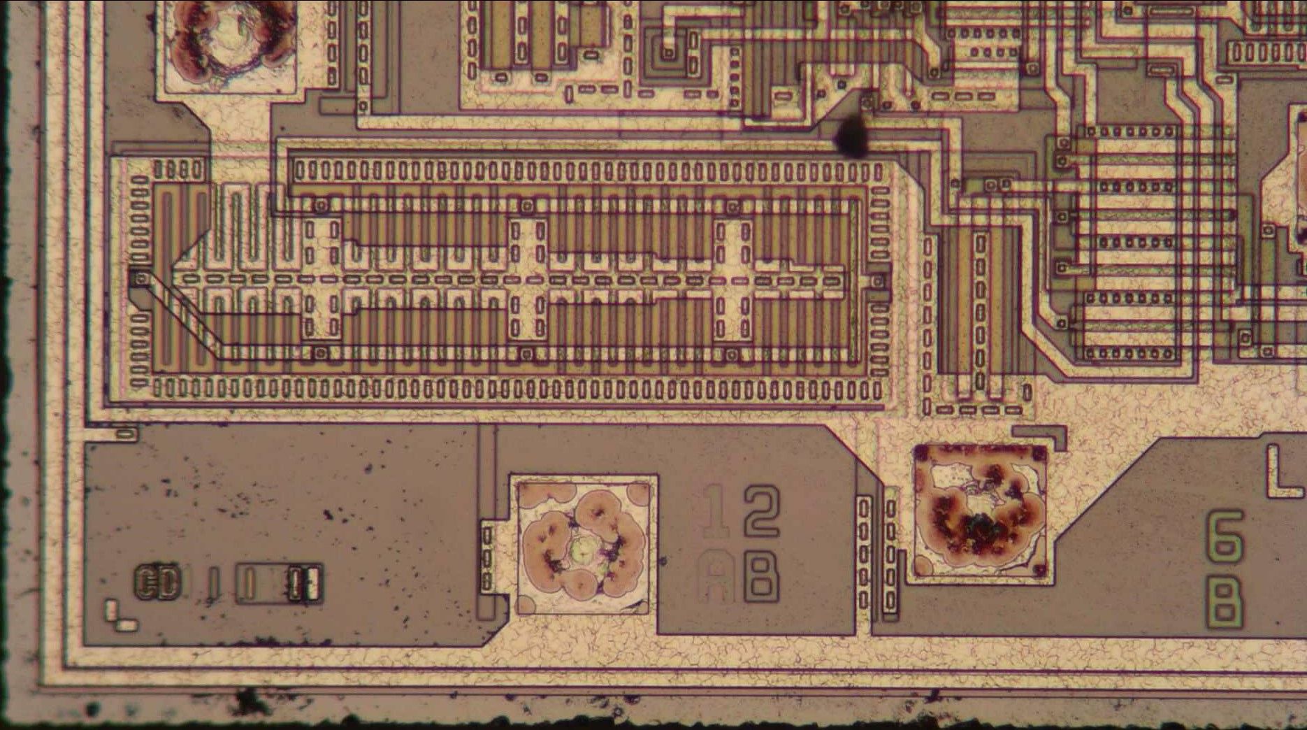
The design is similar to TI’s, with a full-CMOS PTAT current source, but also sheet resistors and a single NPN (T25).
There is plenty of space to place a few layer markers (1A, 2B etc) as well as the chip type (LMC555). We can also see the ESD clamps on all inputs (TRIGGER, THR, RESET and CONT) which are made of two bipolar transistors, one octagonal and one D-shaped. The big output transistors have serpentine gates, like they do in the ST chip.
Also, like in the ST chip, the six resistors are laid out as 1-3-2-4-5-6 to improve their matching.
The LMC555 is also available in an SMD package.
Inside we find almost the same chip, with just a few tiny differences. Most likely, this is the one currently produced, because I bought this specific chip new. The DIP version had been in my parts box for many years and could be more than twenty years old for all I know.
In the lower left corner there’s no longer the UK-F3 designator, but a marker labelled “OD” plus some layer indicators. “OD” typically refers to the diffusion layer that forms source and drain terminals of a CMOS transistor. Interestingly, the other layer indicators show exactly the same version number as in the DIP chip.
The “UK” designator, without the “F3”, has moved to the top right. The copyright date is still 1996. Perhaps NSC just updated the layer designators and didn’t think it worth a full new copyright date.
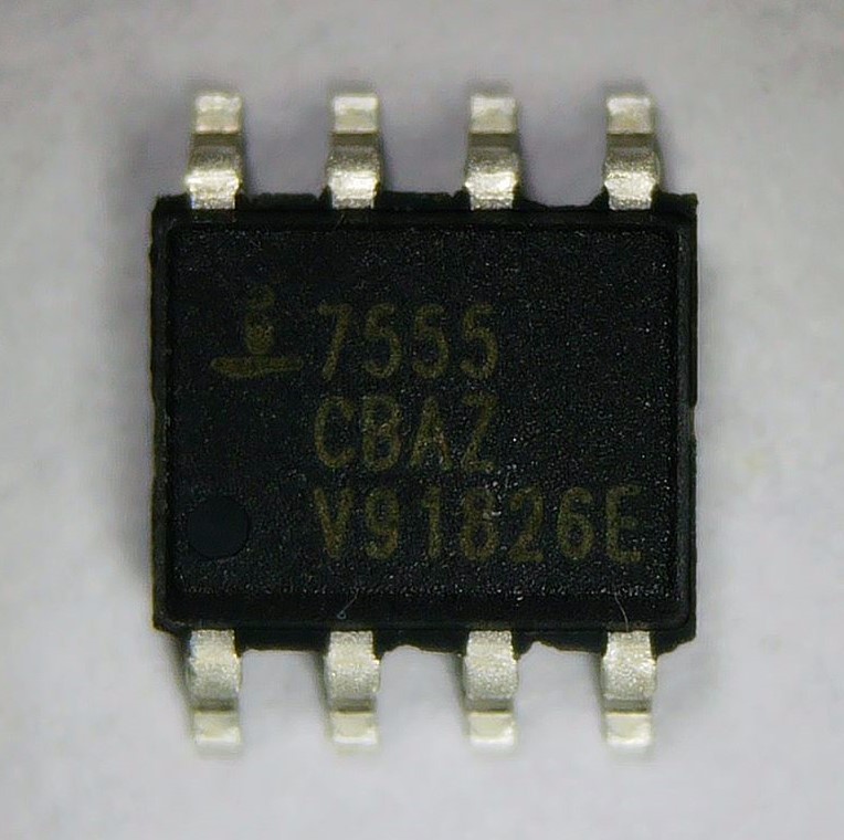
The last CMOS 555 we’ll look at today is Intersil’s 7555.
This chip was apparently designed in 1988, making it the oldest design in today’s batch (although by only one year). The original Intersil company, which was founded in 1967, was taken over by GE Semiconductor in 1980. The combined company was then sold to Harris in 1988, so it’s likely that this chip was developed under GE management and later manufactured under the Harris brand.
An old Intersil data book shows a chip photo that looks similar to what we’ve found, although it’s not exactly the same. This is likely the design as it was between 1980 and 1988, since the databook was published under the name “GE Intersil”.
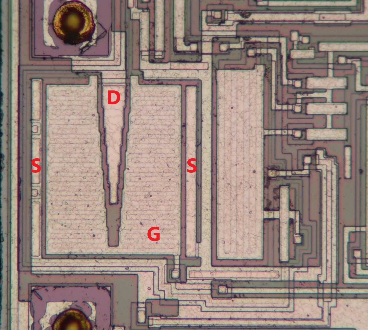
The output transistor has a serpentine gate layout and “Christmas tree”-style source/drain routing. Unlike the TI, ST and National chips, Intersil has placed metal on top of the gates of the larger transistors. We can still see the serpentine polysilicon gate below the metal layer however.
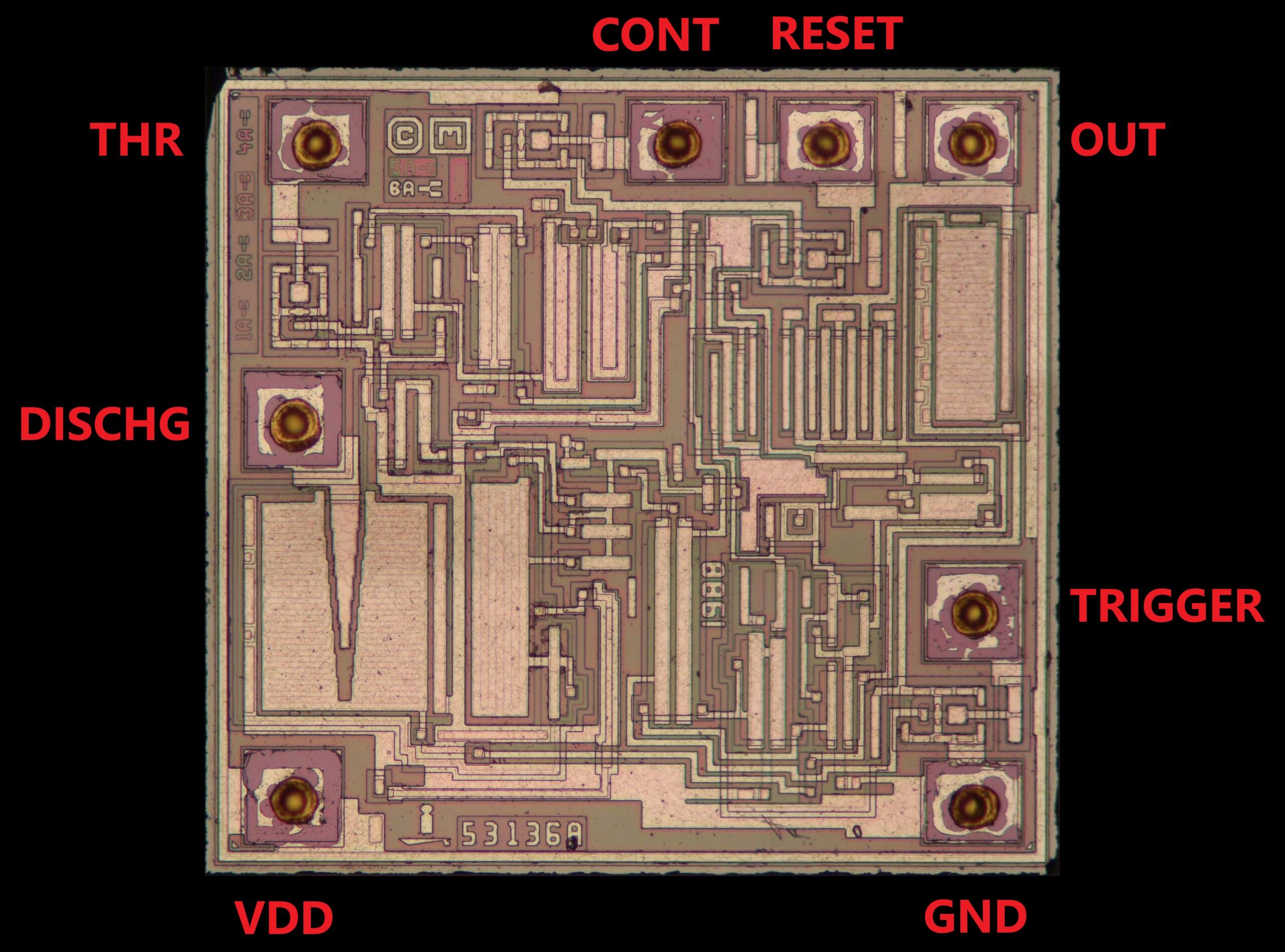
In the top-left corner we find a couple of layer markers which are apparently all revision “A”. We also find the threshold comparator with its differential pair Q1/Q2 and current mirror Q3/Q4. Note how Q3 has two drain contacts, one to connect to Q1 and one to connect to the latch. The sources of Q3/Q4 connect to VDD by contacting an N-well that’s hooked up to the supply voltage. The VDD pin is all the way on the lower left of the chip, and to save on metal, the VDD routing in this part of the chip is done through a well.
Intersil’s engineers didn’t bother to make a neat, matched layout for the three resistors. Instead, they drew two U-shaped resistors side by side (R1 and R2) and streched R3 in an L-shape below it. They even had to use a little polysilicon bridge to for the connection between R2 and R3, which is probably why R2 is slightly shorter than R1. Note also how there’s metal routing on top of the resistors: GND is carried along R3 to the circuits above, and the threshold reference is routed along R1. The wire on top of R2 is connected to its pin B, but doesn’t actually go anywhere.
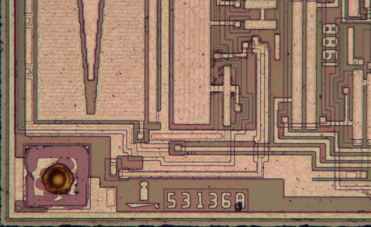
At the lower edge of the chip, next to the VDD pin, we find the Intersil logo and an internal part number “53136A”. The current Intersil company has been part of Renesas since 2016, but the old logo is still commonly seen on products. As we’ve seen with National and TI, there’s often no rush to replace the old logos, especially on older products.