Intel introduced the 80486 processor in 1989, as a successor to the 80386. It provided a significant increase in processing speed: a 486 was about twice as fast as a 386 at the same clock frequency. This was achieved mainly by a pipelined design and 8 kB of on-chip L1 cache. The initial 486 design also included an FPU, which in 386 systems was still an optional, separate chip.
In late 1991, Intel introduced a low-cost version called the 486SX, and renamed the original processor 486DX. The only difference between the two was the presence of the FPU: a 486SX system was much slower than a 486DX when performing floating-point calculations, but was otherwise identical. The absence of an FPU did not make much of a difference for many common tasks such as word processing, and the 486SX became very successful in low-end consumer PCs, displacing the last generation of 386 processors.
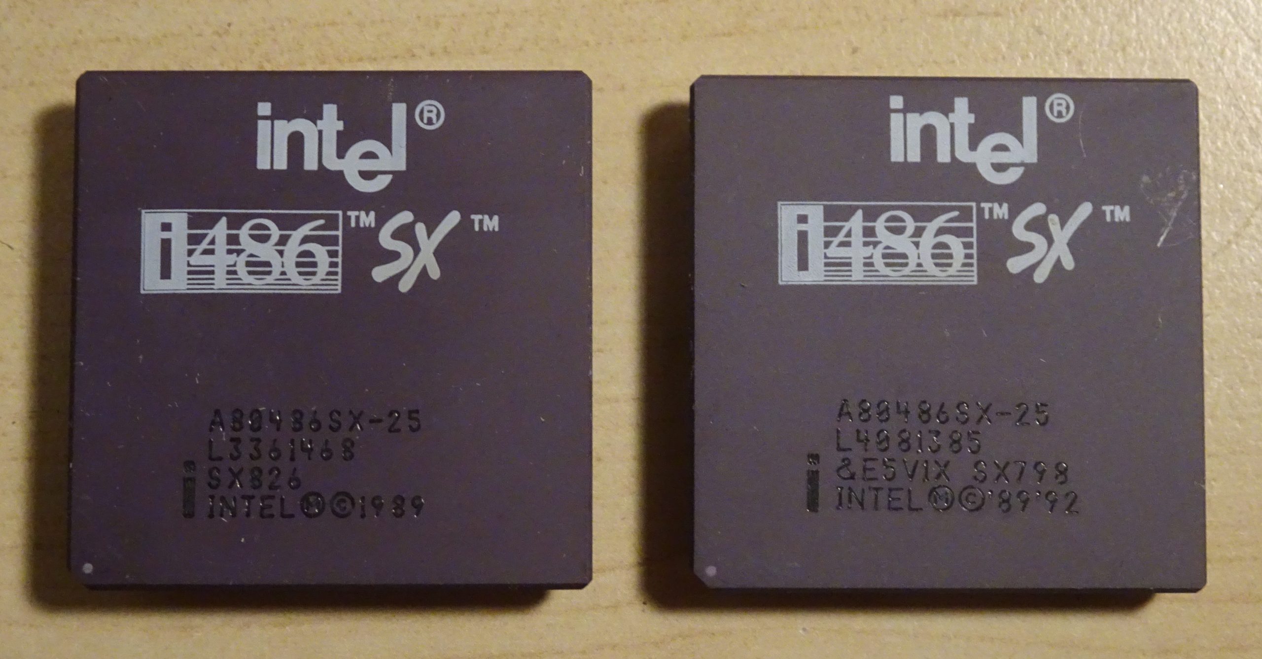
Today we’ll look at two very similar chips. Both are 486SX processors running at 25 MHz. Although the ‘SX was also available in 16, 20 and 33 MHz versions, I’ve found that 25 MHz was by far the most common. I’ve owned several systems with this processor, but since it was so easy to upgrade them to much faster DX or DX2 processors all SX chips quickly ended up in my spare CPU box.
The four lines of text etched into the top of the package tell you what exact version you’re looking at. There are several websites to help you decode the part number [1]https://www.cpu-world.com/info/id/Intel-80486-identification.html, and the only difference between these two is that the one on the right (the newer one, with a 1992 copyright date) is an SL Enhanced CPU, which means that it has power management functionality. The new chip most likely also includes bug fixes and small optimizations.
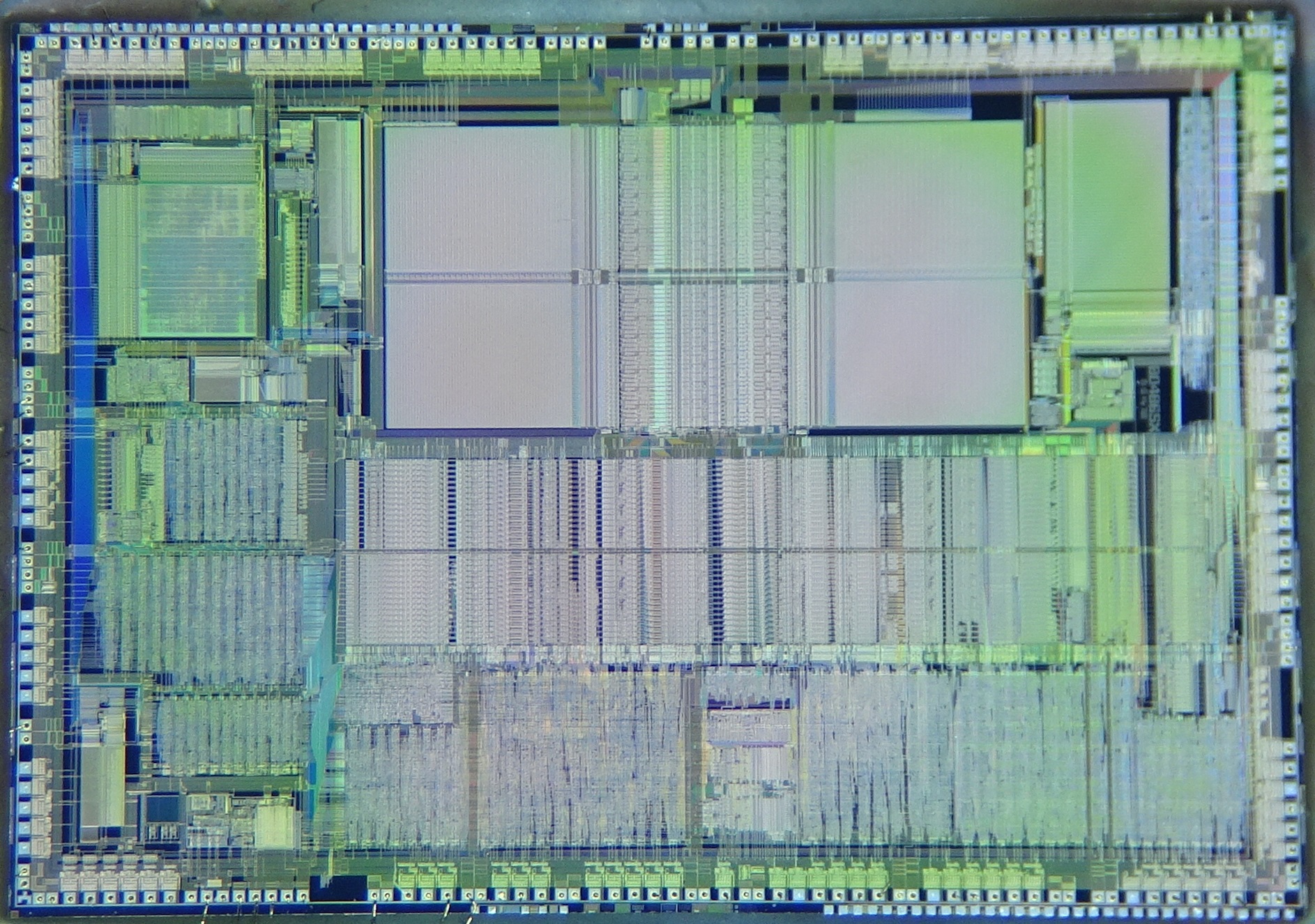
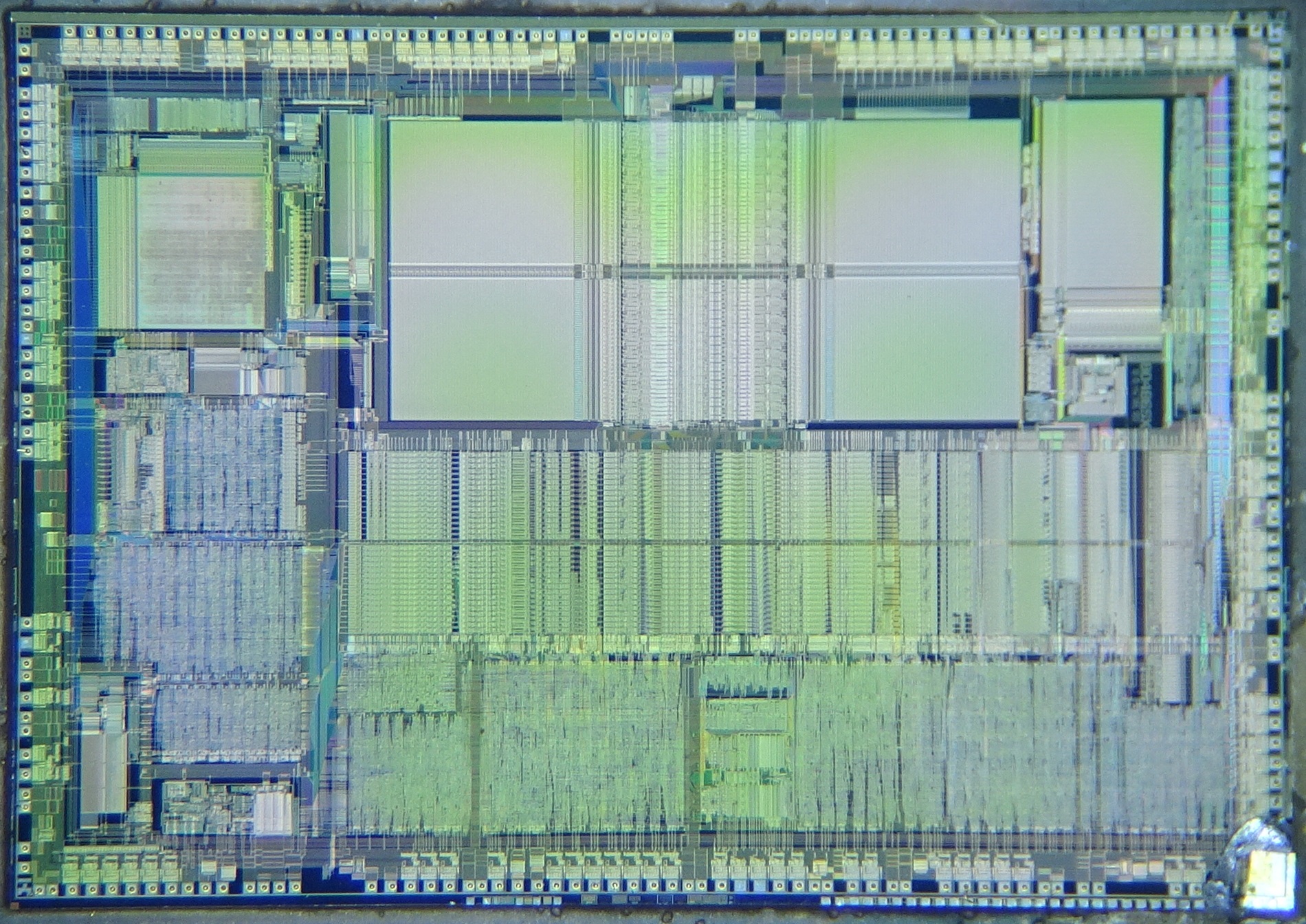
Here is a side-by-side comparison of the two dies. They are remarkably similar; I was expecting the newer one to be made in a different process, to have a more compact layout or to have additional circuit blocks, but in fact the vast majority of the area is identical between the two. It’s also interesting to see that many bond pads are in different locations. I was not expecting this either, since the packages are identical.
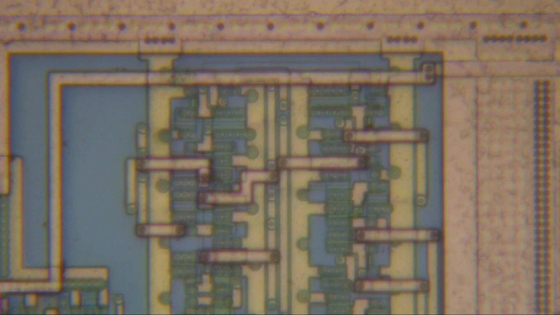
Let’s take a look at a few areas that are different between the two:
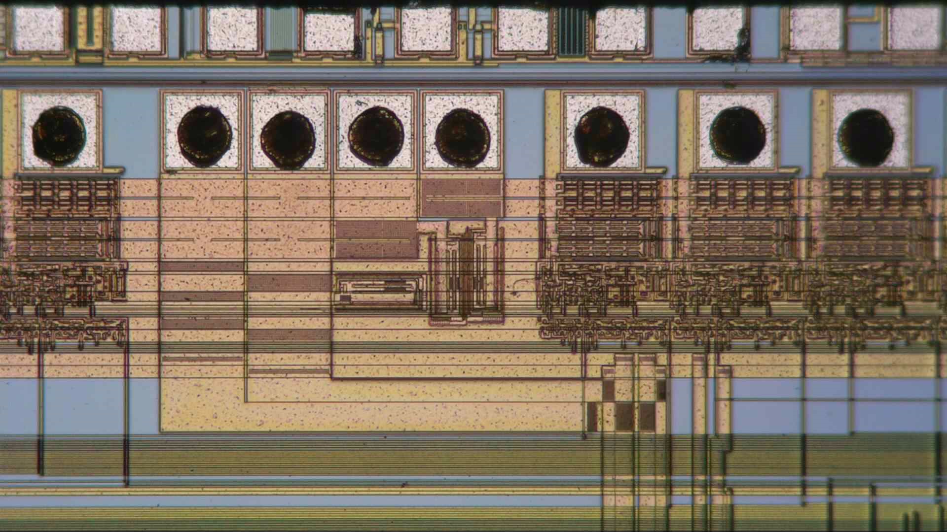
The most obvious difference is in the copyright date. The 486SX was originally introduced in late 1991, so even the 1989 copyright date is somewhat off. Note how the circuits on the left are identical, while on the right side a new block of transistors has appeared in the newer chip.
At the lower left corner of the chip, we find a block that’s present in the old chip, but missing in the new one. This block contains three similar copies of what looks like an analog circuit with a very large resistor. Why the new chip didn’t need it is anyone’s guess; it could be that we’re looking at a complex power-on reset circuit which was deemed unnecessary in the new revision. Or perhaps the same functionality was implemented in the small circuit block on the left side of the new chip (partly on top of the large metal traces).
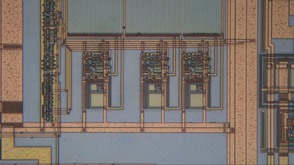
Zooming in on the old chip, it clearly looks like three identical copies of some analog circuit, connected to three very large resistors on top.
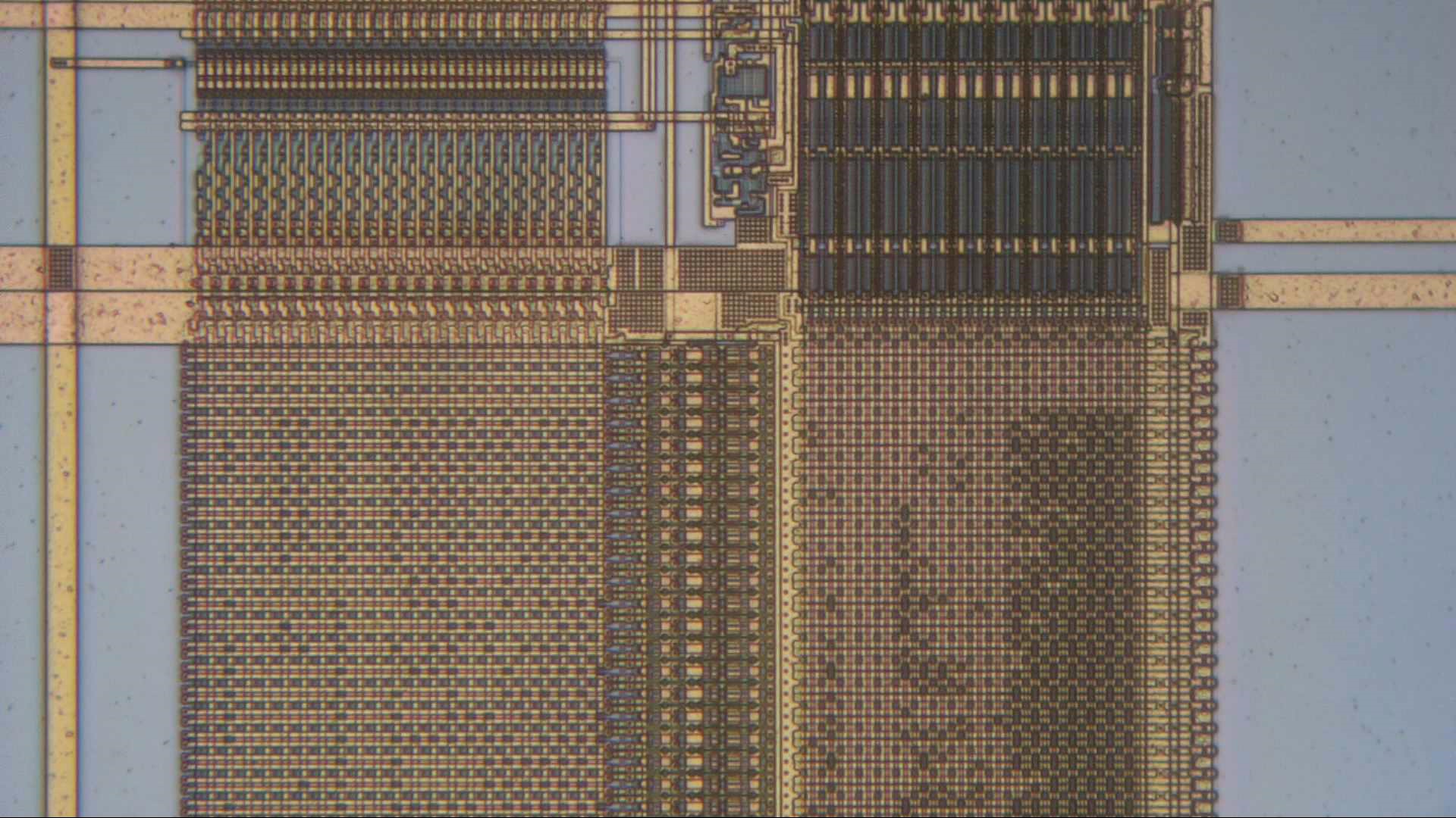
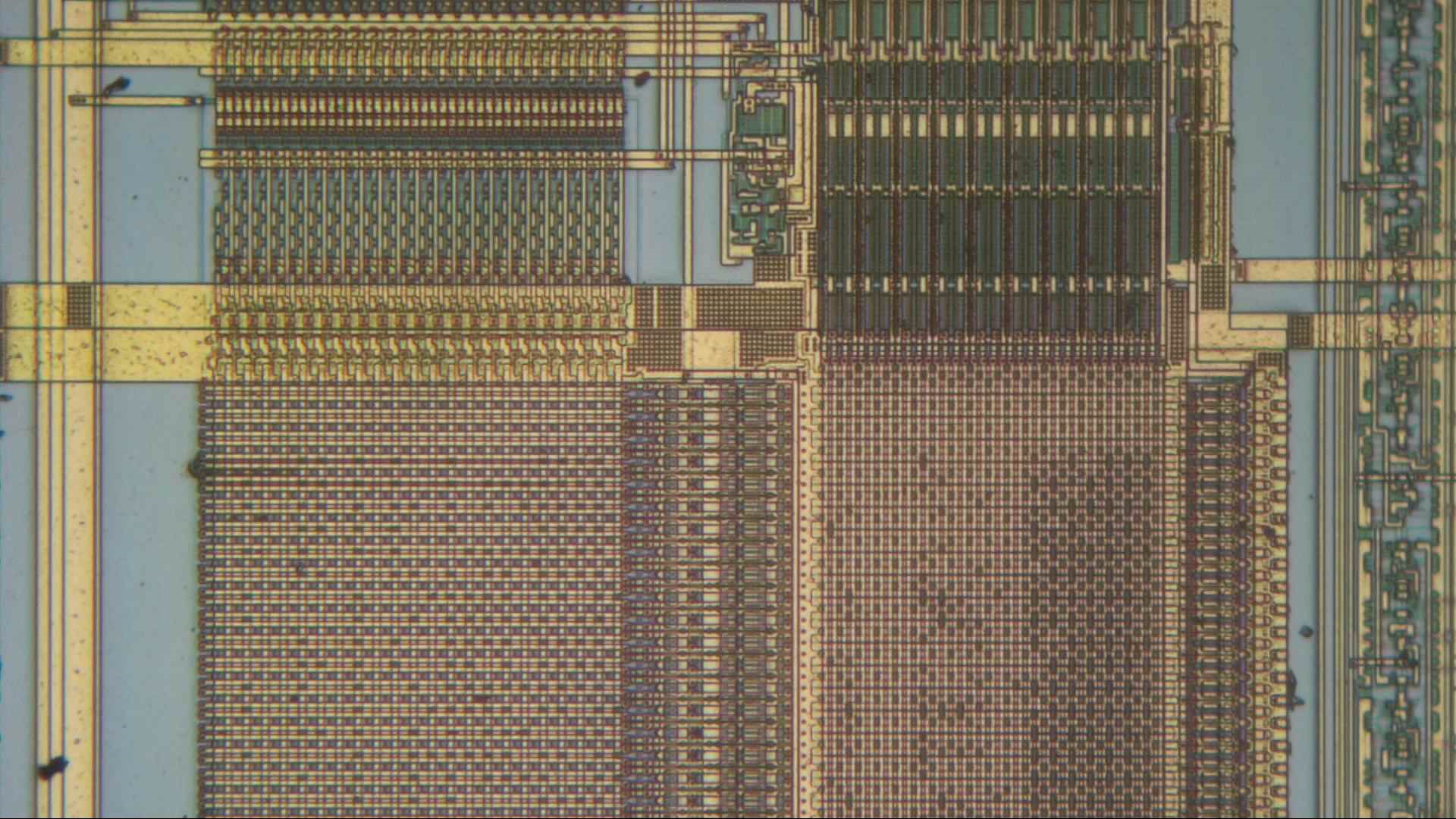
Here we’re looking at a piece of ROM inside the two processors. The overall structure is the same, except for the vertical structure just to the right of the memory. My guess is that this allows the chip to turn off power to the ROM when it is in power-saving mode. The ROM contents also appear to differ between the two chips.
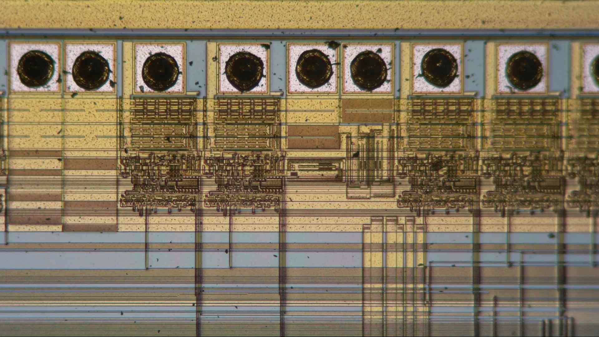
One oddity about the two chips is that the pad ring (where the die connects to the package) is not the same. Generally there is quite a bit of flexibility in the placement on the chip, while the layout of the package is largely fixed. Since these two chips share the same package one would think their pads would be in the same place, but nearly all of them have shifted. On the older chip we also see a row of (smaller) probe pads right on the edge of the die. The fact that the new chip doesn’t have them doesn’t mean much: often these test structures are scattered across the wafer, and not even all chips cut from a single wafer will have identical structures at their edges.
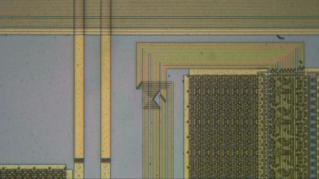
A funny thing that’s identical on both chips is this bundle of wires. In the middle of this picture, you can see that four wires, out of a bundle of six, make an odd U-shaped jump, apparently to shift the order of the wires. This looks like a typical last-minute wiring fix, which is often something you’d try to fix properly in a new revision, but it seems the engineers at Intel didn’t think it worth the effort.
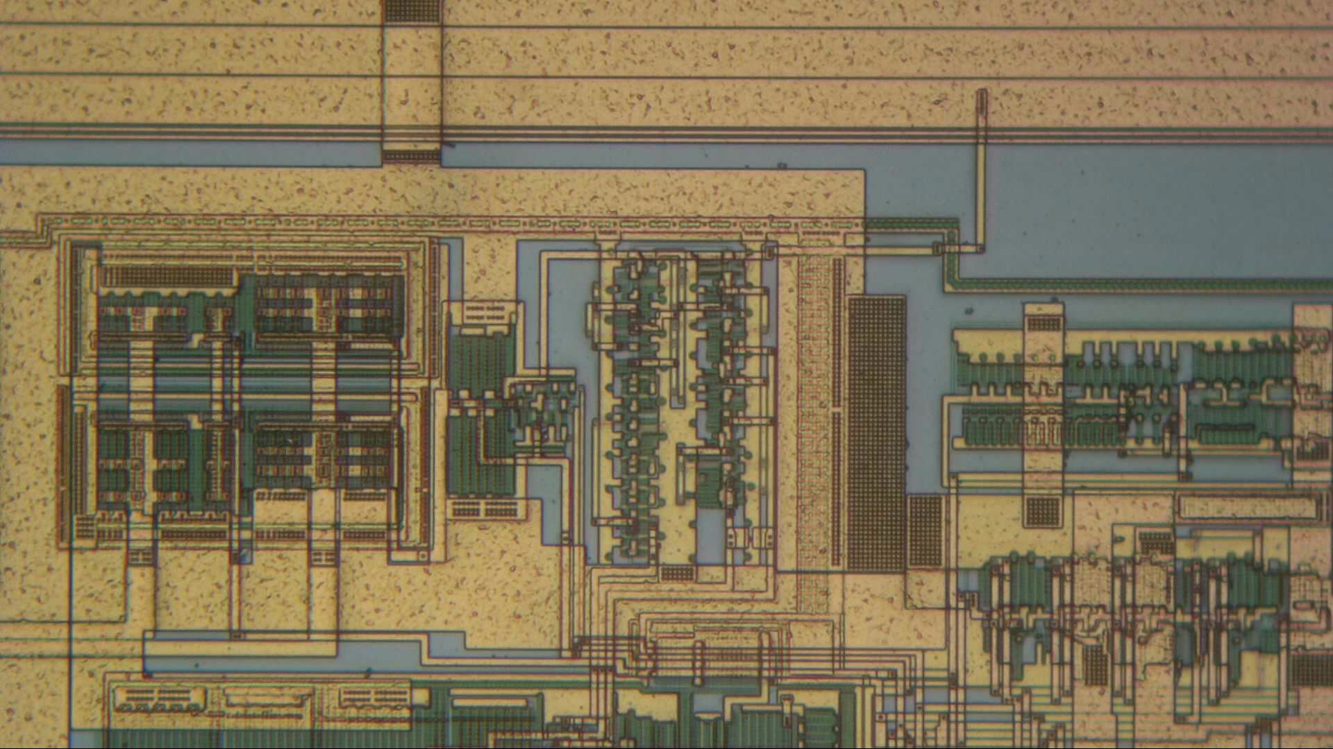
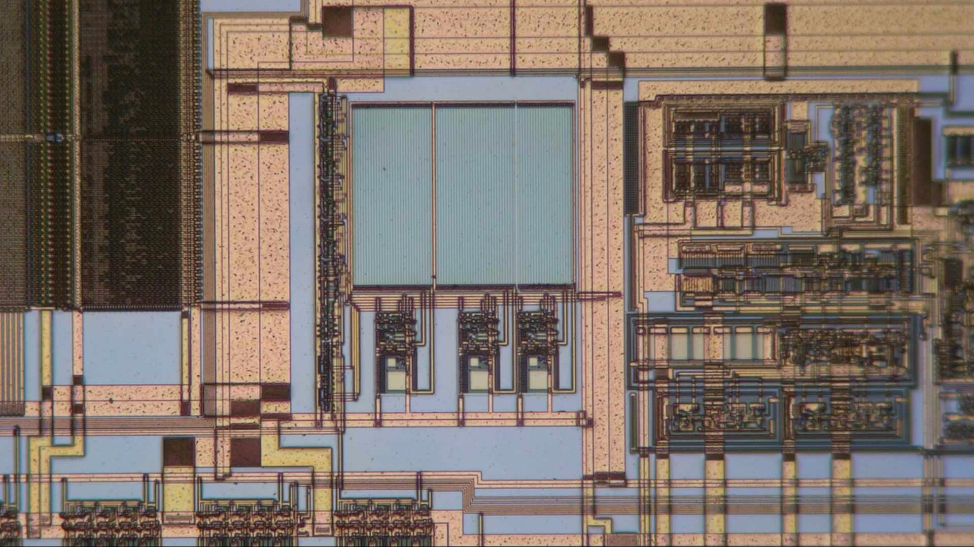
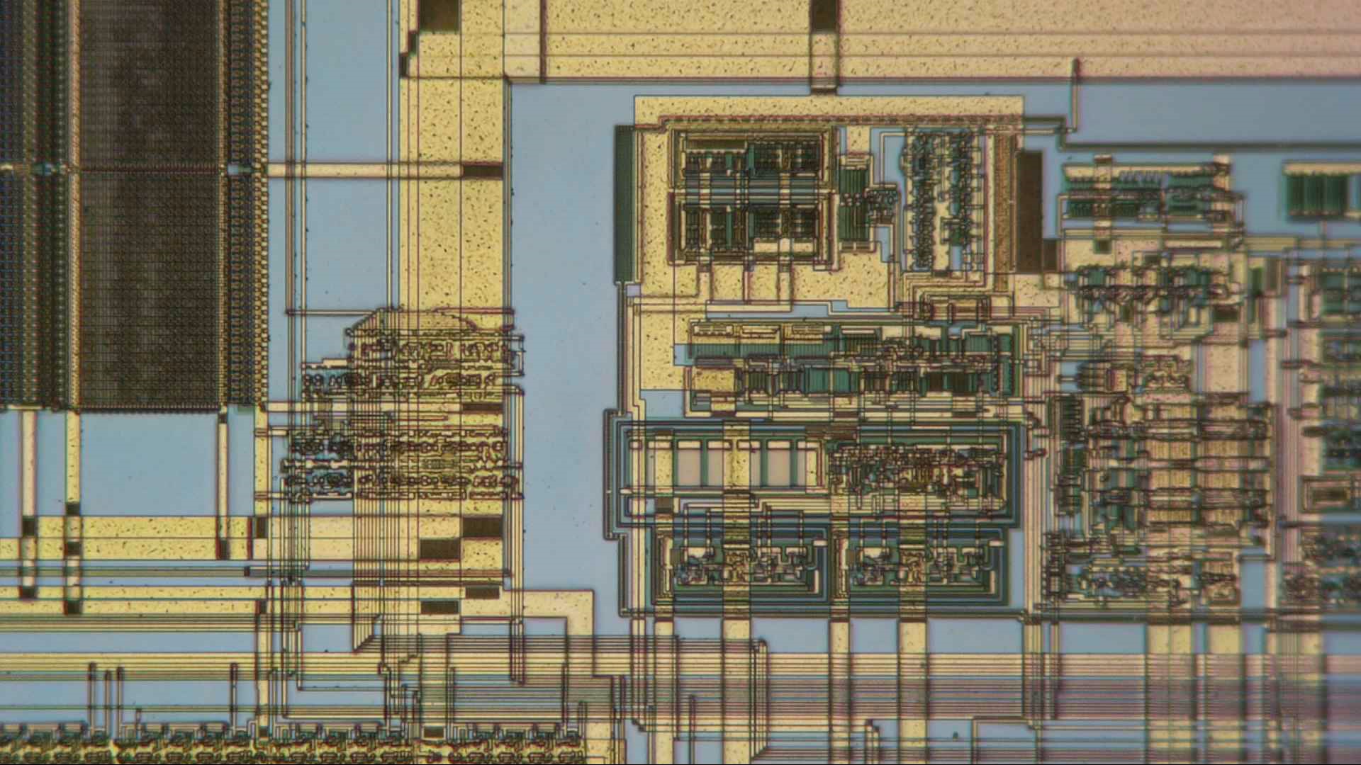
Going back to the lower-left corner of the new chip, I’m zooming in on this rather interesting-looking piece of circuitry. We see lots of wide metal traces, large transistors on the left and a wide variety of different circuits all around.
Zooming in even further, we can actually see a piece of CMOS logic. The vertical bars in the middle are the supply line, while those to its left and right are ground. In between them are NMOS and PMOS transistors. The manufacturing process of these 486SX chips only had two metal layers, which means that it would be the P648 process [2]https://en.wikichip.org/wiki/intel/process. Later versions of the 486 family were made in the more advanced P650 and P652 processes, which had three and four metal layers, respectively.
Back in the 1990’s when Star Trek: A Final Unity was coming out, I remember reading about it in a gaming magazine. I was prepared to soon upgrade my 386 to a 486SX. After reading in the magazine that the new game would require a 486DX2, I changed my mind and had the computer upgraded to a 486DX2, just so I could play this game.
Apparently from what I remember, I read something somewhere that the DX2 had a math co-processor that would be required for the game, something that the SX didn’t have.
I doubt that a math co-processor would really be required for a game; in the ‘386 and early ‘486 era they were far from standard equipment in consumer-grade PCs, so any game that required them would find its market somewhat limited. A point-and-click adventure like Star Trek: Final Unity would definitely not need a co-processor.
In any case, if you wanted to have a co-processor you’d need just a regular 486DX instead of a 486SX, because that was basically the only difference between the two. But a 486DX2 would definitely be the better choice for any use case, since it had effectively twice the computing power because of its doubled internal clock speed.
A Final Unity’s system requirements did, in fact, state that the floating point co-processor was required. Apparently, it would still work without it, but with reduced performance.
Here’s an excerpt from Wikipedia’s page on the game:
“A Final Unity officially required a floating-point coprocessor (FPU), which was unusual for MS-DOS games at the time. It could still be played on a computer not equipped with one, but at reduced performance.”
in my first PC I had a 486SX25, though I didn’t play Final Unity, but I didn’t meet any game at that time that had a problem due to the lack of a coprocessor. BTW I ran this processor with 40MHz clock without any cooling – I didn’t even have a heatsink on it. These days it would be sold as a 486SX60 with a heatsink and a fan 🙂
My first cpu with 33MHz ❤️🥰