If there’s a classic analog chip even more iconic than the 741 op amp, it has to be the 555 timer. Released just three years after the 741, it similarly took the world by storm, selling billions of units over five decades. Quite unlike the 741, which established op amps as a common IC type, the 555 has remained largely in a class of its own. There are many ICs that can generate square or triangle waves, but I can’t think of any chip that can function as a one-shot, a flip-flop, Schmitt trigger, or one of a million different oscillator types like the 555 can.
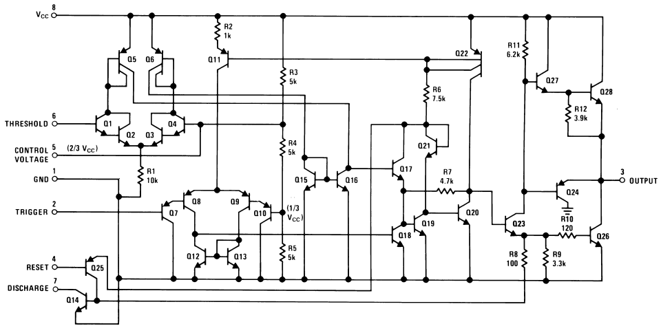
Designed by Hans Camenzind in 1972, its story is described in detail in Camenzind’s own book Designing Analog Chips. I highly recommend reading it (available on paper or as a free download) if you’re interested in analog IC design. In Chapter 11, Camenzind shows the schematic of the original 555 timer:

It’s a rather clever setup with two dozen transistors forming two comparators, a flip-flop and an output driver. Originally released by Signetics, it was quickly copied by most other semiconductor manufacturers of the day. Today I’ll show a couple of them, starting with the oldest one I found in my collection: a TDB0555DP by Thomson.
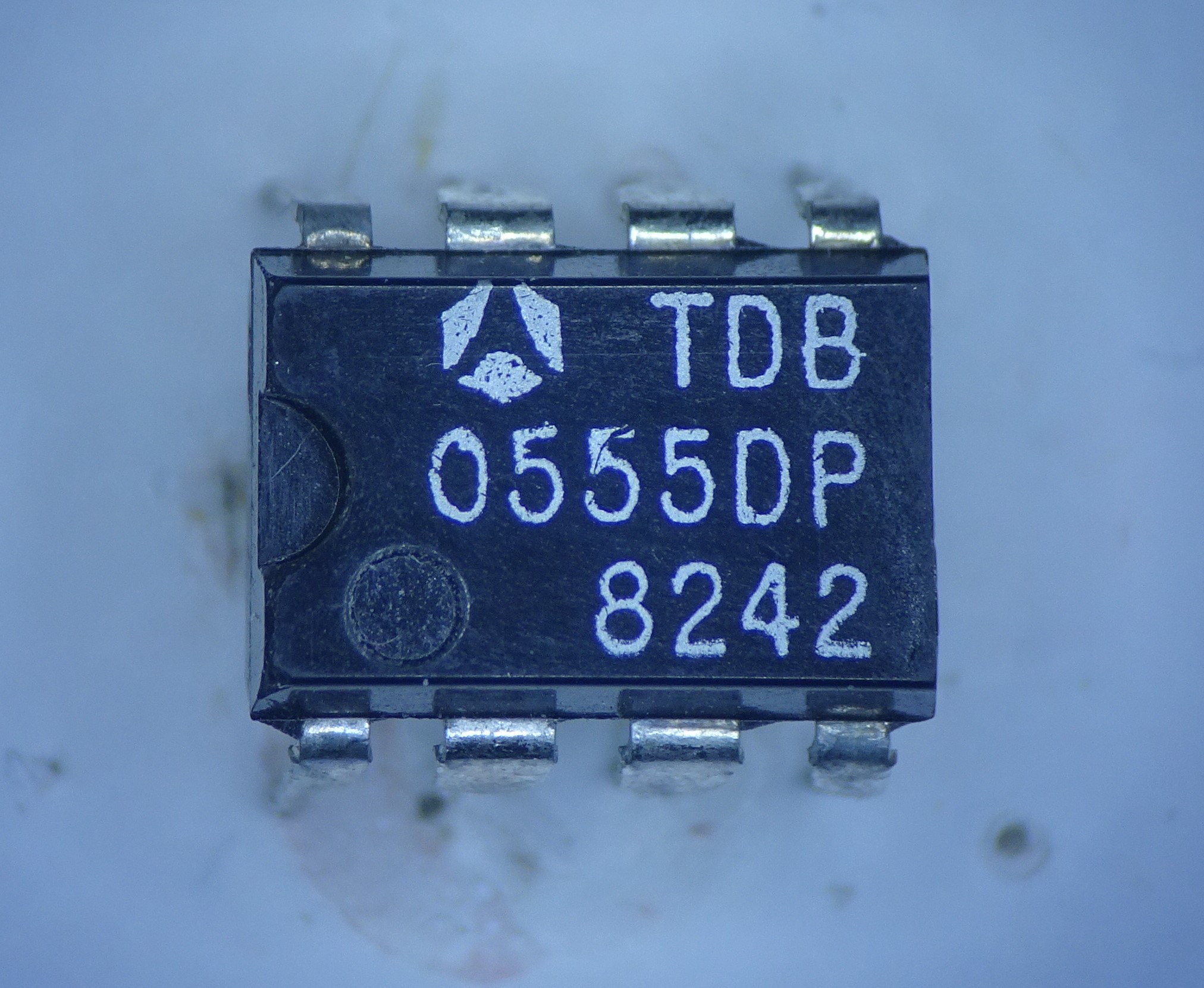
This chip has a 1982 date code. Thomson (a French company) long ago merged with SGS of Italy to become STMicroelectronics, which is one of the largest semiconductor manufacturers today.
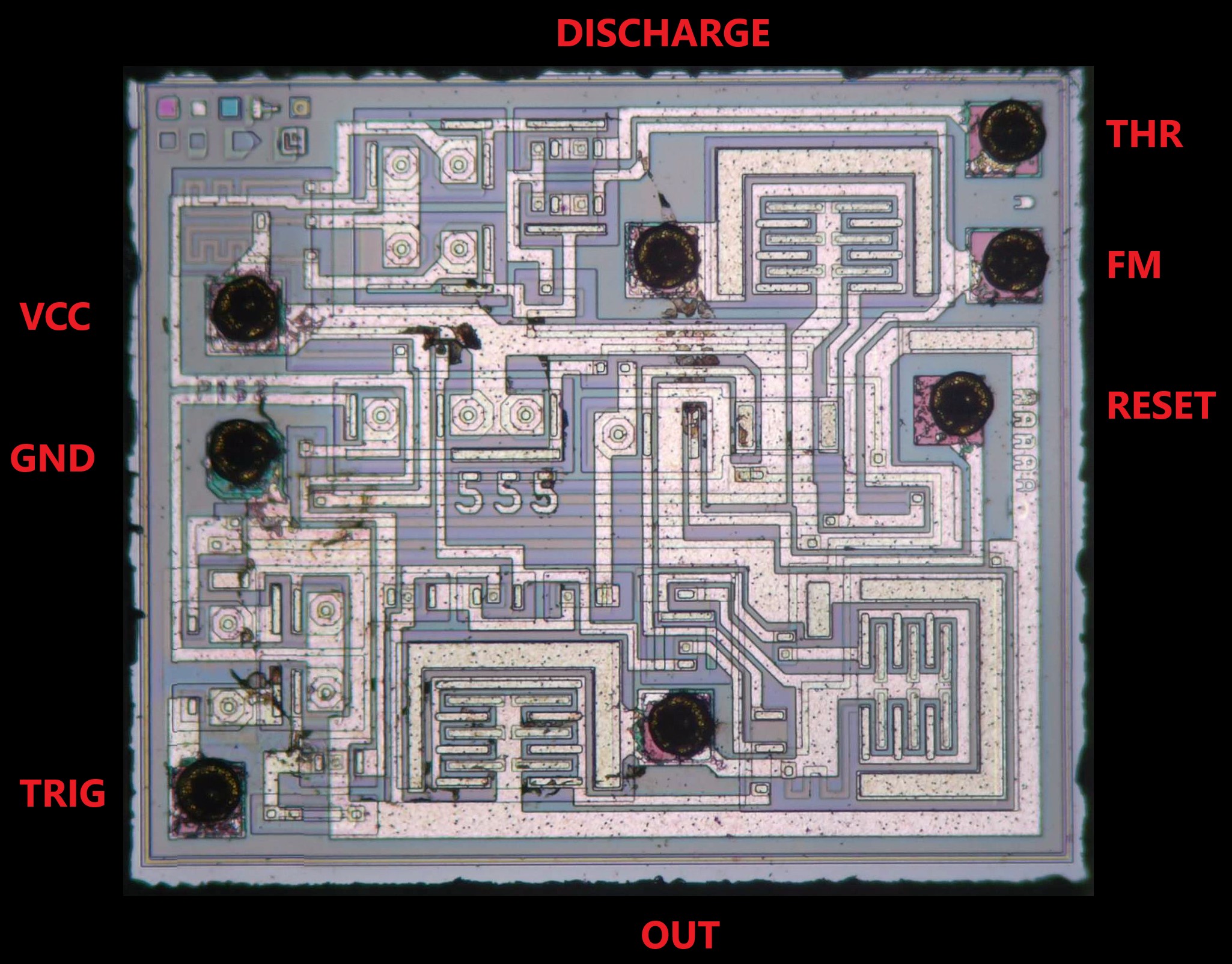
Inside we find three large 5s showing the chip’s function. But there’s no manufacturer logo or other identifying information other than a barely visible “P152” between the VCC and GND pins. On the right edge is a row of As showing that each mask is in its first revision. The top left corner has a number of colourful test patters.
Note that the “555” numbers are sitting on top of the three 5 kOhm resistors R7-R8-R9 that span almost the entire width of the chip. Also clearly visible are three very large NPN transistors: the two output transistors (Q22-Q24) on either side of the output pin, and the discharge transistor (Q14) next to its own bond pad.
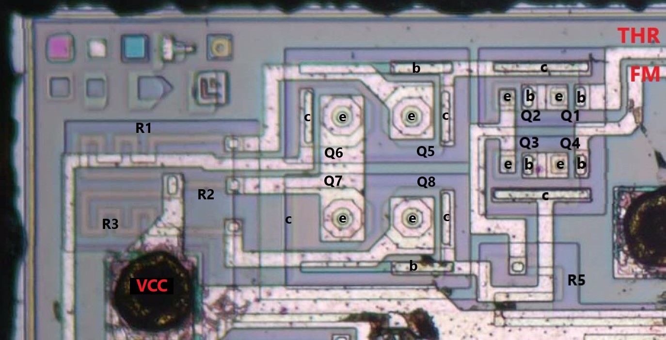
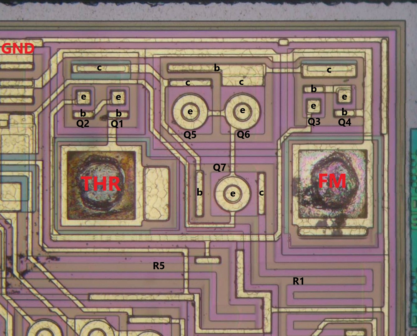
Zooming in at the top-left corner, we can clearly see the Threshold comparator. I’ve labelled the transistors to match Camenzind’s schematic. The NPN Darlington pairs (Q1/Q2 and Q3/Q4) share a single N-well, as do the PNP current mirrors (Q5/Q6 and Q7/Q8). One interesting thing to note is the collector of Q7: it needs to connect to ground, but instead of attaching a collector contact and routing it to the GND pin using a metal wire, this chip’s designer decided to simply extend the collector’s P-diffusion to the edge of the N-well, so it directly contacts the P-substrate. This does mean that Q7’s current flows through the substrate towards the nearest contact. If that happens to be far away, there could be a significant voltage drop which pushes up Q7’s collector voltage.
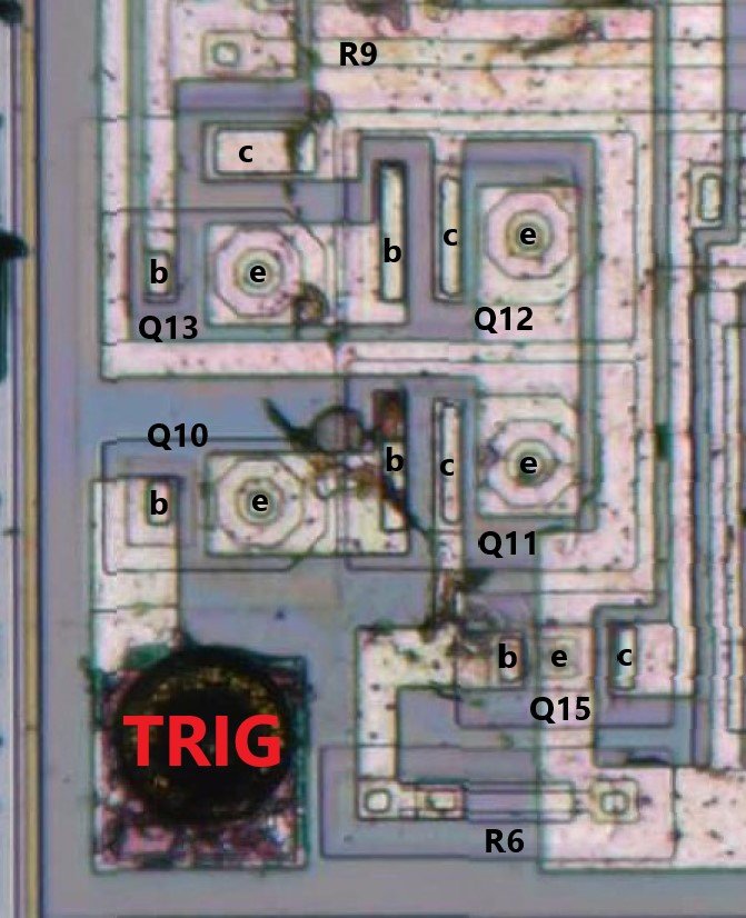
Here is the trigger comparator, and again we see the exact same components as in the schematic. Q10 and Q13 are in fact vertical PNPs, which can be used at this location since their collectors are connected to ground. Note that there is a substrate contact nearby to ensure the collectors are connected through a low resistance. Q11 and Q12 are lateral PNPs. R6 is a pinch resistor, recognizable by the outline of the emitter diffusion on top of a (narrow) base diffusion. This makes it possible to squeeze 100 kOhms into such a small area.
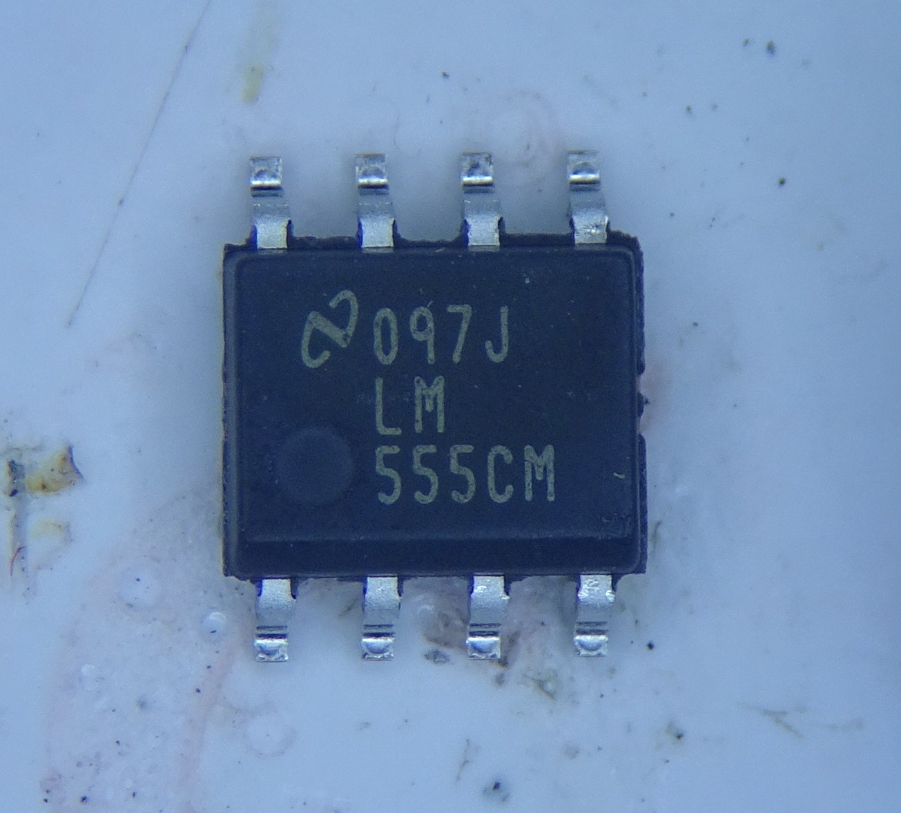
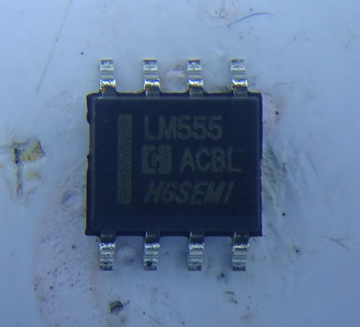
Next up is National Semiconductor’s LM555. NSC was acquired by TI back in 2015, but the old logo still lingers on classic products that you can buy today (as we saw earlier on the LM741).
National’s clone of the 555 is rather unusual, because it actually contains a few significant changes to the circuitry. Below is the schematic as printed in the datasheet.
Starting at the Threshold comparator, we notice that R1-R2-R3 are missing. Although Q5 and Q6 are drawn differently than in Camenzind’s schematic, they are actually connected in the same way. This is because removing the emitter resistors makes it possible to turn the two PNP current mirrors into split-collector PNPs, which saves space compared to having four separate transistors.
The output of Q5-Q6 goes into an NPN current mirror, Q15-Q16. An emitter follower (Q17) then feeds the signal into the flip-flop. The NPN mirror gives additional gain to the comparator, because it uses both polarities of the differential signal coming out of Q5-Q6 and drives it into the high-impedance node at the collector of Q16. In the original design this gain was achieved by the ratio of R1-R3 over R2, while Q7’s signal was simply dumped into ground.
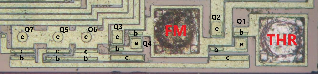
A second difference is in the Trigger comparator. Instead of R6, National’s designers chose to implement another NPN current mirror, Q12-Q13. This should give this comparator more gain as well, ensuring a cleaner switch-over and lower offset. How much all of this helps is unclear though, because the specs on National’s datasheet are identical to those of all other 555s….
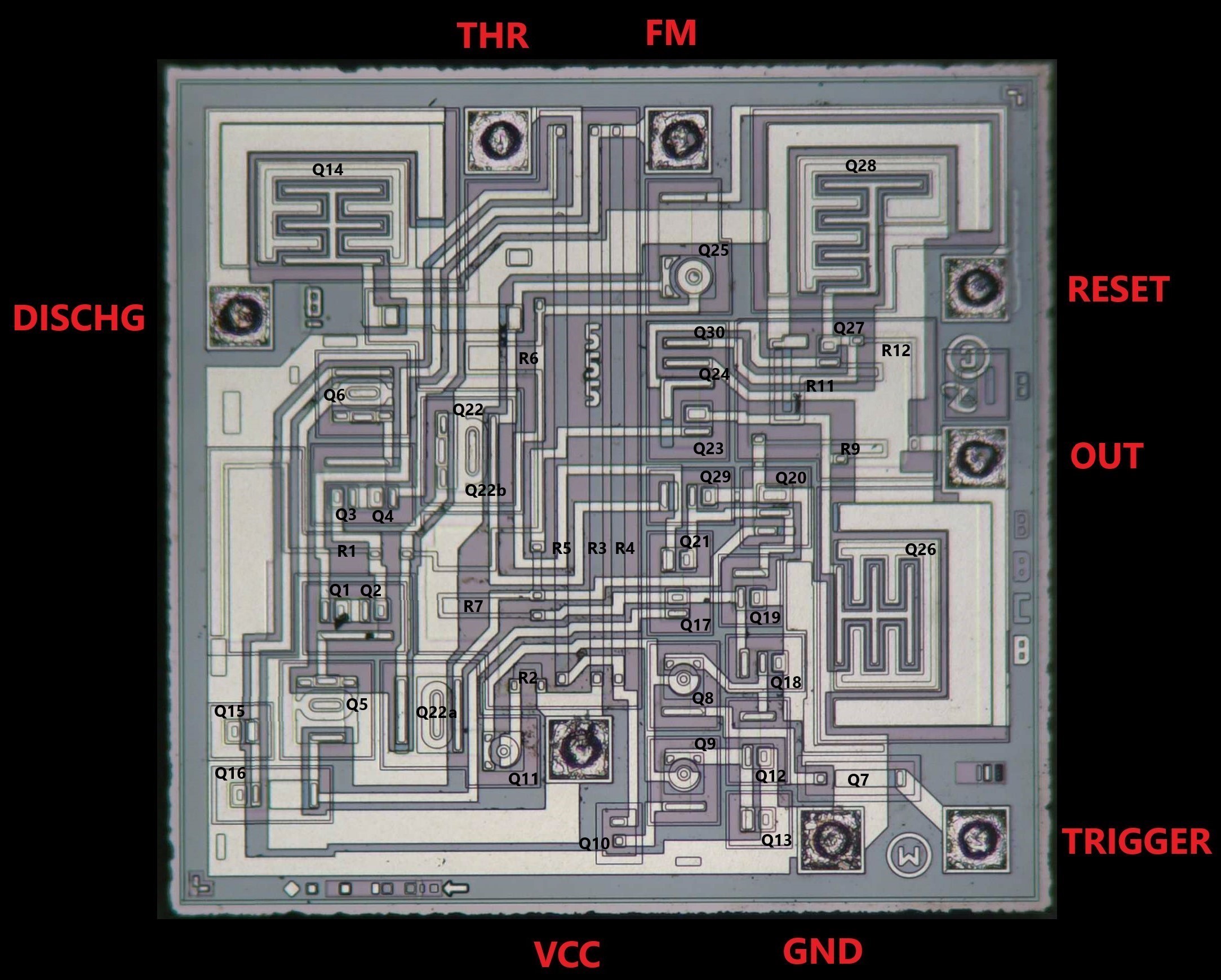
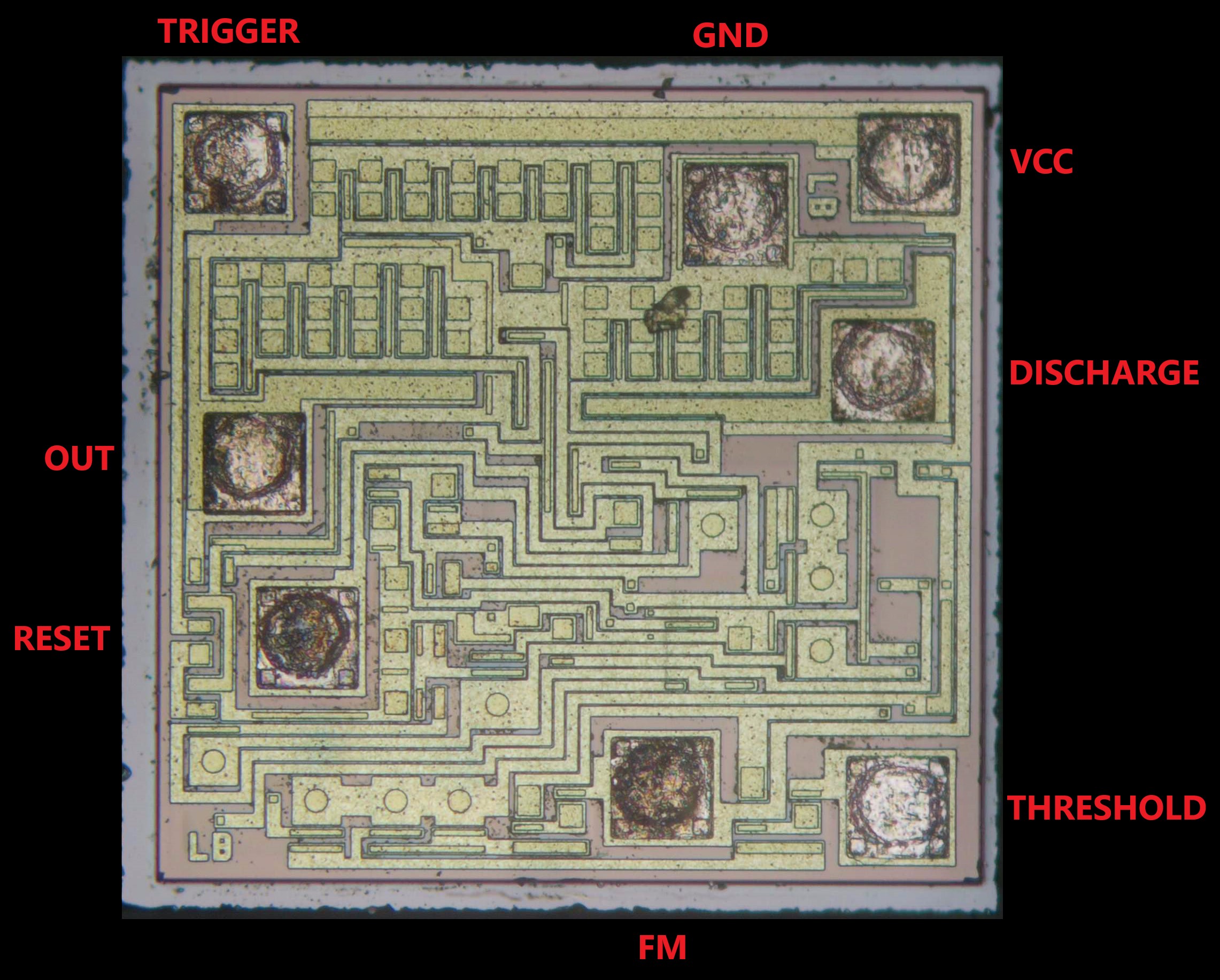
Inside we see again the numbers “555” on top of the three resistors, the Discharge transistor at the top-left and the output transistors on the right side of the die. National did include their corporate logo as well as the Mask Work and Copyright marks. Interesting to note is also that all masks are at revision “B”, while one is even at revision “C”. Apparently it was necessary to do a complete redesign at some point.
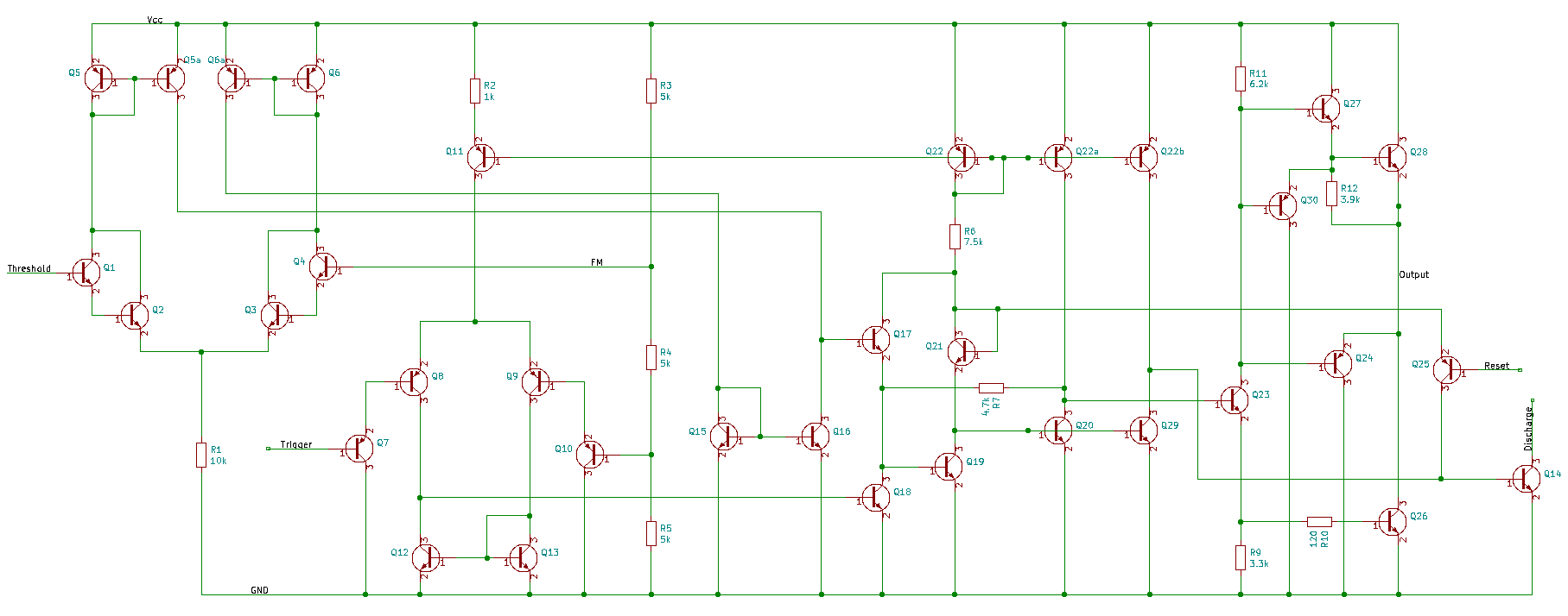
I’ve annotated the layout above with the labels from National’s schematic. As it turns out, this chip does not exactly match the drawing: there are two more transistors, which I’ve labelled Q29 and Q30. Also, Q22 is split into two separate transistors, one of which has a split collector, for a total of three current branches instead of two. I’ve drawn the complete schematic below.
For some reason, National decided to drive the base of the Discharge transistor (Q14) from a separate current branch Q29-Q22b. Perhaps this was done because Q14 can draw more base current than Q20-Q22a can deliver.
Another small difference with the datasheet schematic is Q30 (a vertical PNP, like Q24). Together with Q27 this forms a totem-pole driver to drive the base of Q28, which enables Q28 to turn off more quickly: in the original design Q26 would drive Q28’s base low through R12.
Note that Q24 is also implemented differently than in Camenzind’s design: its collector is tied to ground, not to the collector of Q23. This means that when Q26 struggles to pull the output low, Q24 will start drawing current from the output by itself, rather than feeding extra base current into Q26.
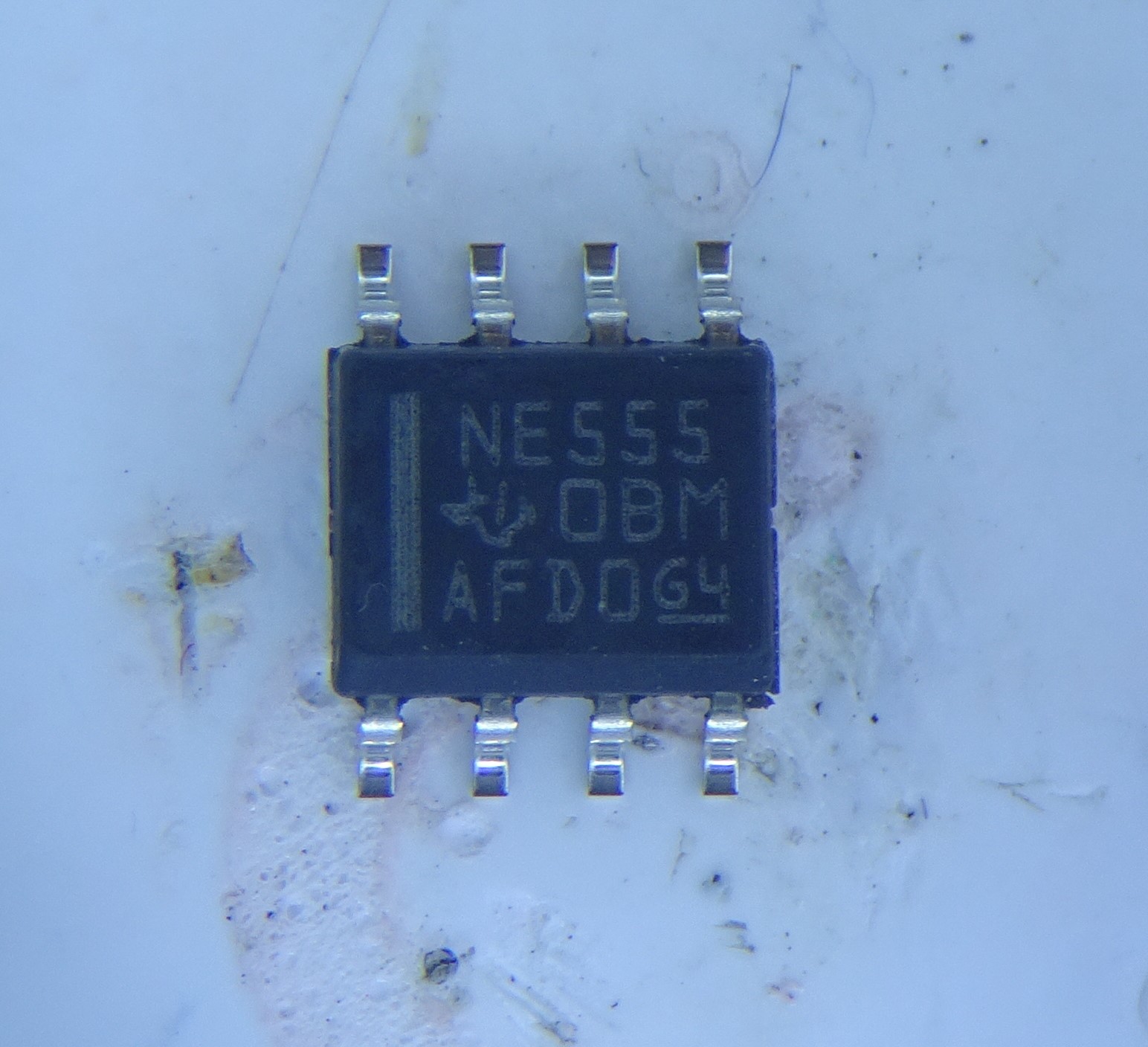
Our next candidate is the NE555 from TI:
Like the UA741 and LM741, TI keeps both the old National chip and its own “native TI” design in production. TI’s datasheet doesn’t show a transistor-level schematic, just a block diagram, so we’ll have to dig into the chip’s internals to figure out what circuit topology they’ve used.
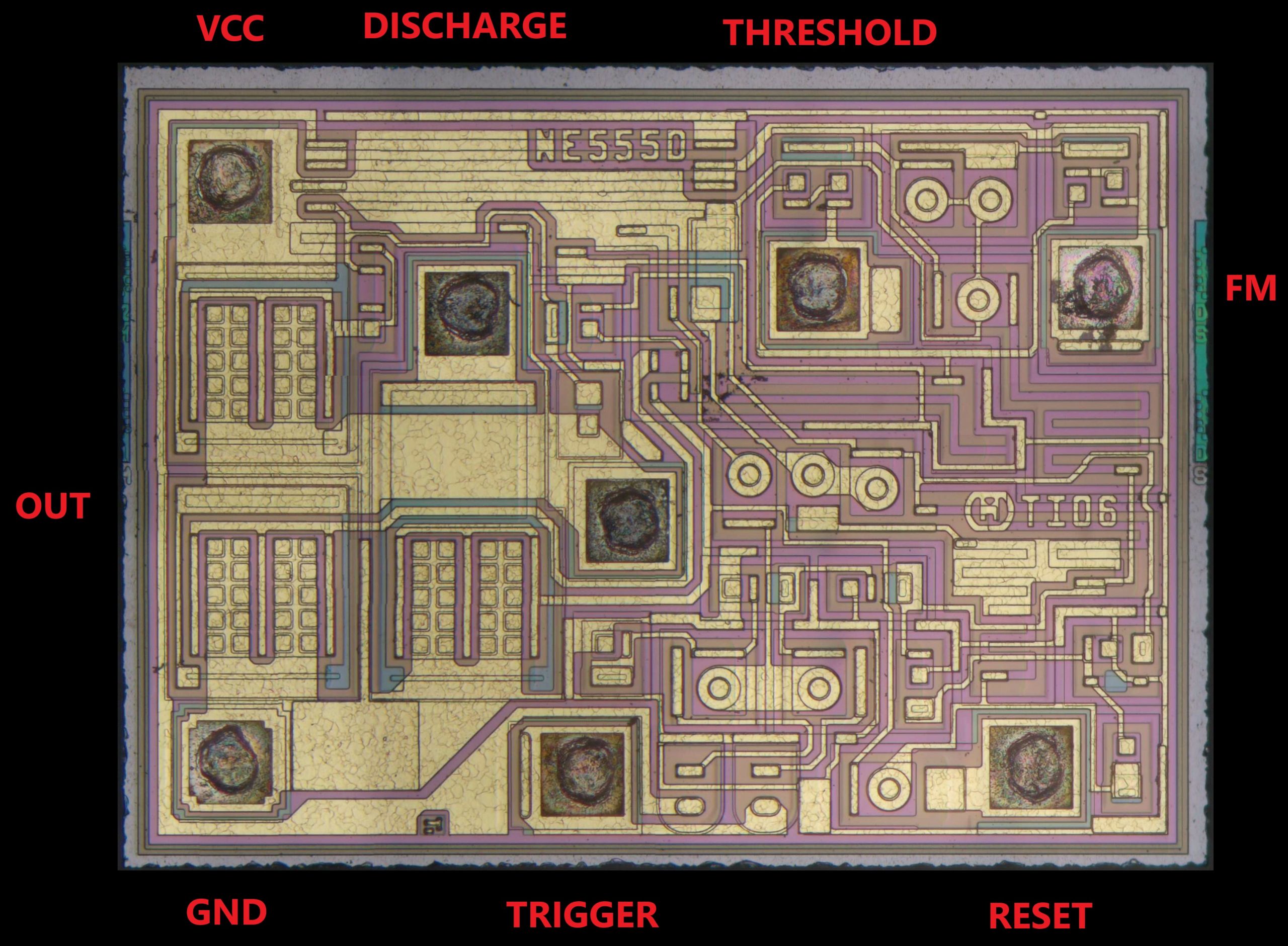
The overall layout looks good, with the three power transistors on the left and circular PNPs on the right. TI has even placed bond pads right in the middle of the die, which is quite rare. It looks like they claim a 2006 copyright date, which would mean they performed a significant design change relatively recently. An older version of the datasheet shows the chip’s metal layout (though still no schematic) and it doesn’t match this layout at all. Possibly TI had to change to a different production process and decided to update the design for this.
After tracing the layout I’ve come up with the following schematic:
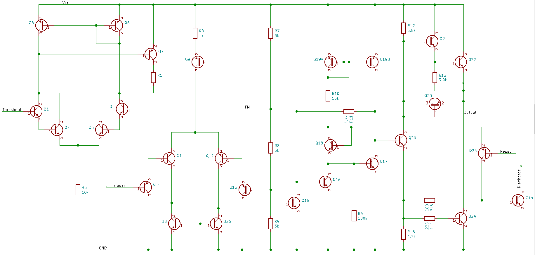
Overall, the circuit matches the original 555 design very closely, but a few things are different. Let’s have a look at the Threshold comparator:
Like in National’s LM555, there are no degeneration resistors. But instead of adding an NPN mirror, TI’s engineers chose to place a PNP mirror (Q5-Q6) directly on top of the NPN darlingtons and use it to drive a PNP common-emitter stage (Q7). This is actually the most obvious way to do it in today’s technology; emitter degeneration is a technique from discrete design, where matching of transistors cannot be guaranteed. In an integrated circuit we can easily make a good current mirror with transistors only. In fact, if Q7 runs at the same current density as Q5-Q6, then the collector voltages of all three transistors are identical as well, which further improves matching.
On the Trigger comparator TI used the same trick National did, replacing the 100 kOhm load resistor with an NPN current mirror. For some reason however, Q17 is now equipped with a base pull-down resistor. Given that it’s a pinch resistor, its value is probably in the range of 100 kOhm. Other than this, the circuit is identical to the original 555.
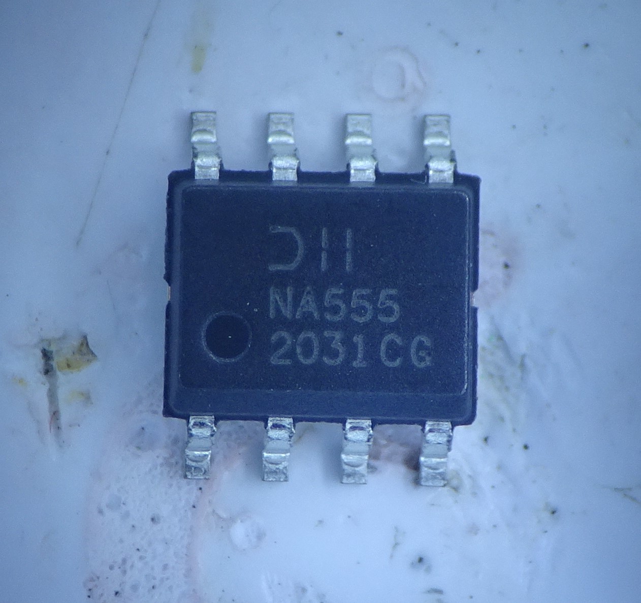
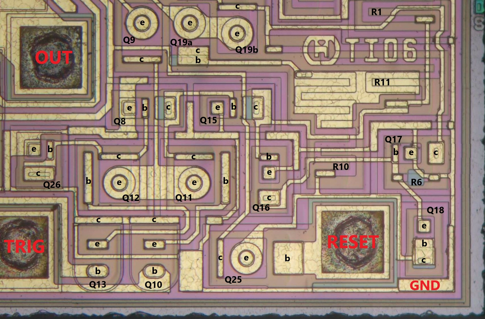
Diodes Inc, of Plano, Texas, also makes several versions of the 555. This is the SOIC version of their NA555. Like TI, Diodes doesn’t include a transistor-level schematic in their datasheet.
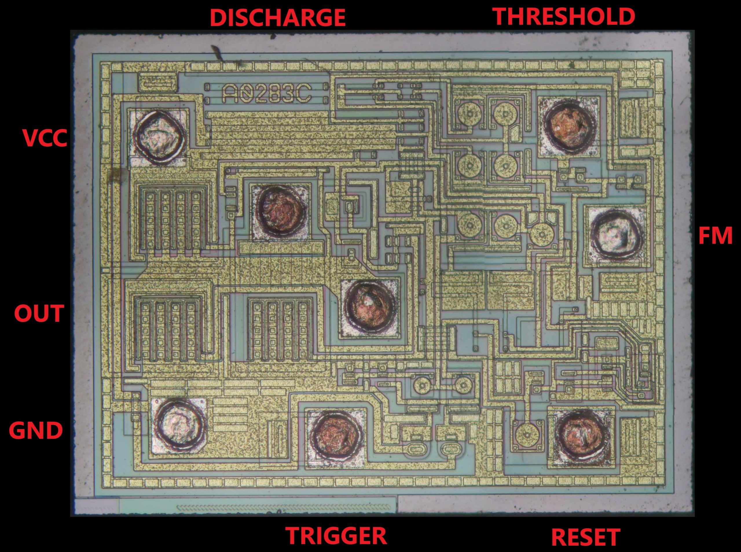
The die doesn’t contain any clear indication of its function or origin. Only the identifier “A0283C” is visible. What is interesting however, is how similar the layout is to that of TI’s NE555. The overall positioning of components is nearly identical, although the manufacturing process is clearly different.
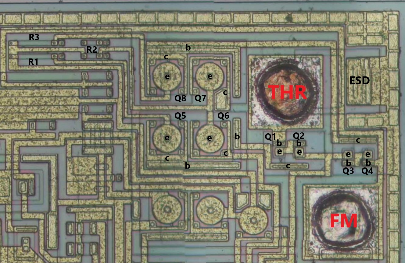
The Threshold comparator is exactly as in Camenzind’s original schematic. A few things stand out: first, we can clearly see an ESD clamp connecting the Threshold pin to GND. ESD clamps were not generally used in bipolar ICs because all the diode junctions effectively work as clamps already. CMOS circuits with their glass gates are much more sensitive to ESD and therefore always include clamps on all external signals.
The second interesting feature of this chip is that all resistors have two contacts on one end, only one of which is used. This makes it possible to increase the value of the resistors by about 10% by changing the metal mask, which might be necessary if the exact value of the resistors turns out to be a bit on the low side.
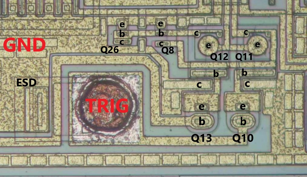
The Trigger comparator uses the same topology as TI and National, with an NPN current mirror (Q8-Q26) loading the darlington PNP input stage. We again see an ESD clamp attached to the bond pad. Another thing that’s common on modern ICs but was rarely seen in the ’70s is a substrate contact ring around the entire chip. This ensures the substrate has a low-resistance path to ground all across the chip, which helps protect the IC against latch-up (although that’s usually less of an issue in bipolar ICs than in CMOS).
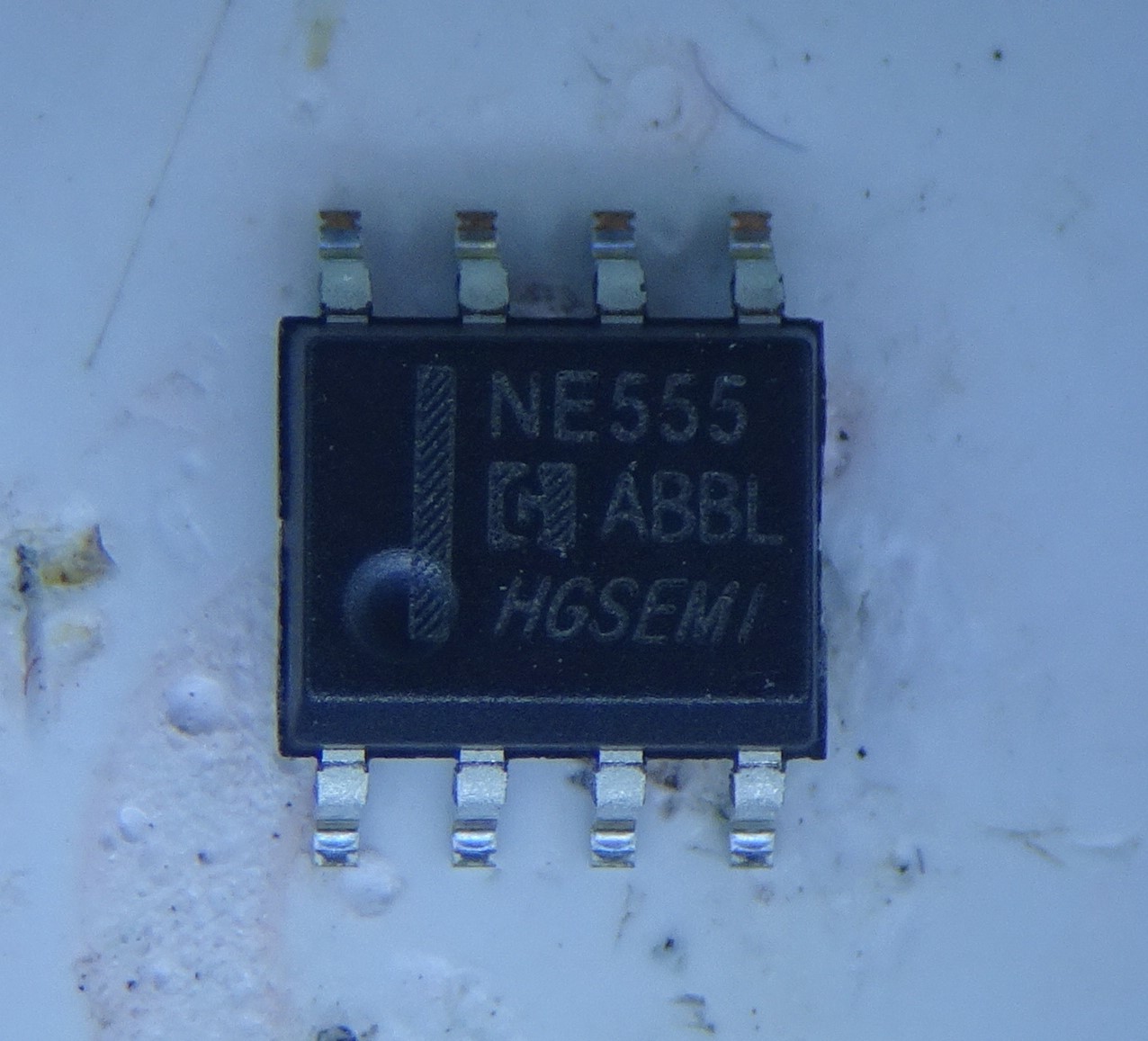
HGsemi, a Chinese manufacturer, also makes an NE555 (as well as an LM555, as we’ll see below). Its datasheet is a blatant copy of TI’s, and HGsemi didn’t even bother to remove TI’s name except on the front page.
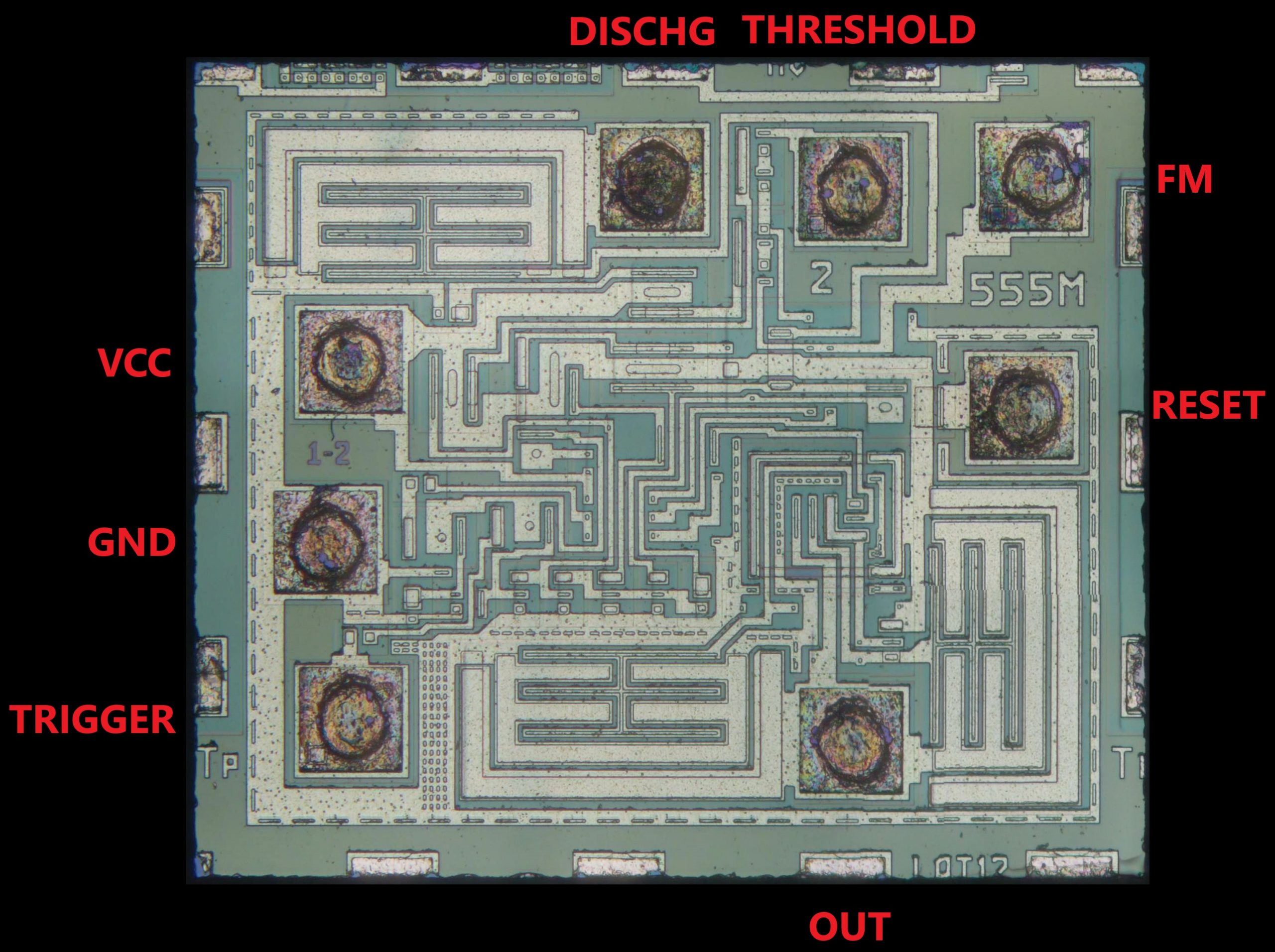
The chip itself is a custom design however. The metal layer is full of right angles; no round transistors here. There are also the remains of test circuits visible on the outer edge.
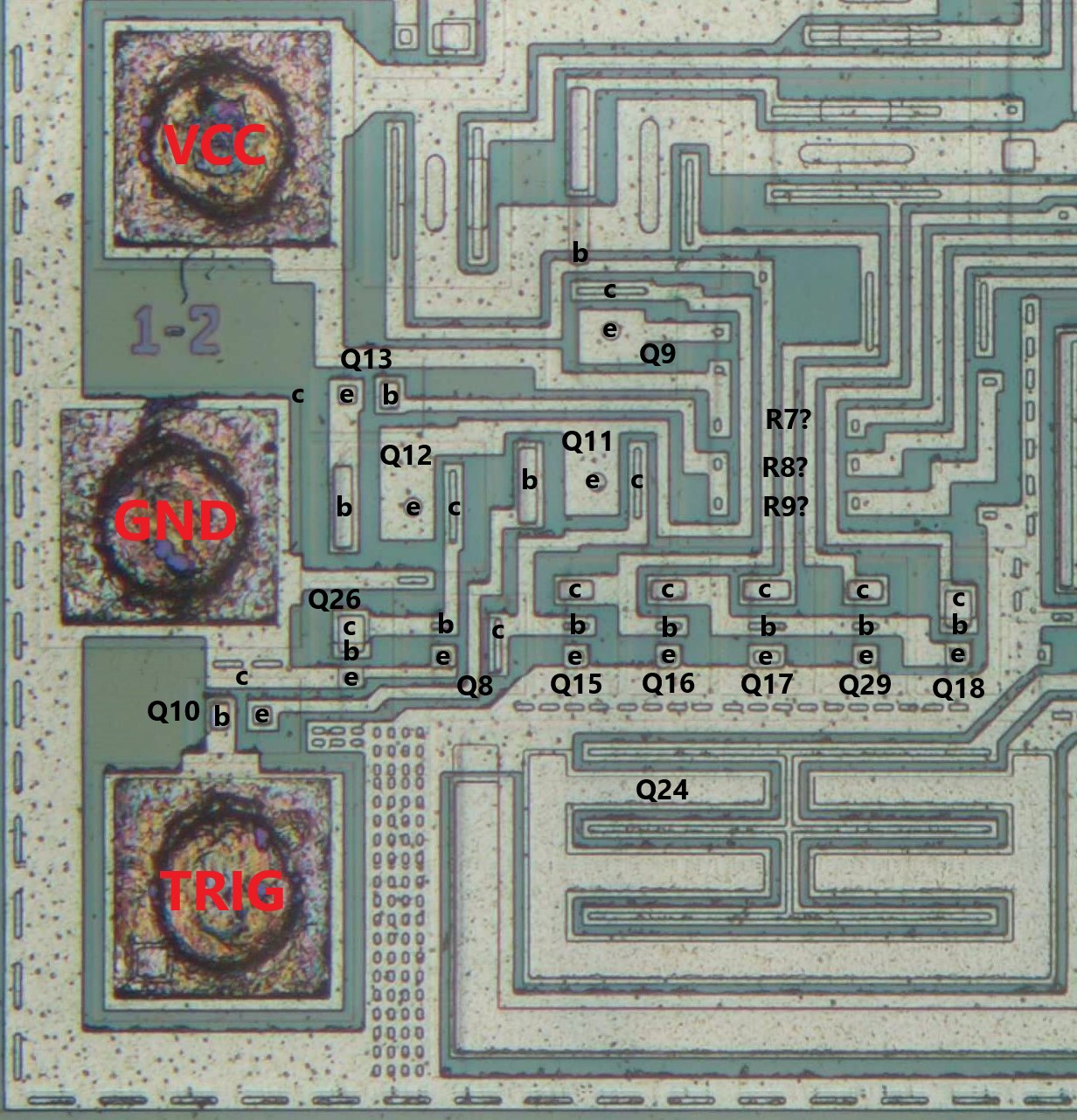
The trigger comparator is again of the type we’ve seen more often, with the NPN mirror (Q8-Q26). Interestingly, this chip also has the separate bias branch (Q29) for the discharge transistor, like in National’s design.
For some reason the diffusion layers are very hard to see in this manufacturing process. Based on the rest of the circuit, the three 5k resistors (R7-R8-R9) should be somewhere below that thick bundle of metal lines, but I can’t figure out where exactly they are located, or even where their metal contacts are.
Overall, this circuit seems to be a copy of National’s LM555. We even see the weird setup with Q24 and Q30 in the output driver. So it’s kind of funny that HGsemi sells this chip as an “NE555”, not an “LM555” which they also have:
It looks identical to the NE555, and one might wonder why HGsemi even bothers to have both in their portfolio. After all, the numbers in the datasheets are identical. HGsemi did make a separate datasheet for the LM555 as well, this time copying the one from ST’s NE555 and replacing “NE” with “LM” everywhere.
Inside it’s actually a different design than the NE555. It really makes you wonder why HGsemi went to all the trouble of designing two different chips which have identical specs. They might as well have made one design to sell under both part numbers… We’ve seen before that they didn’t bother to make a separate design for their “LM741” and instead just relabelled a vaguely similar opamp.
The Threshold comparator is the same design as TI’s, with the PNP mirror (Q5-Q6) directly on top of the NPN darlingtons. The wiring is extremely dense, making it hard to see the devices below. Again the resistors are almost invisible.
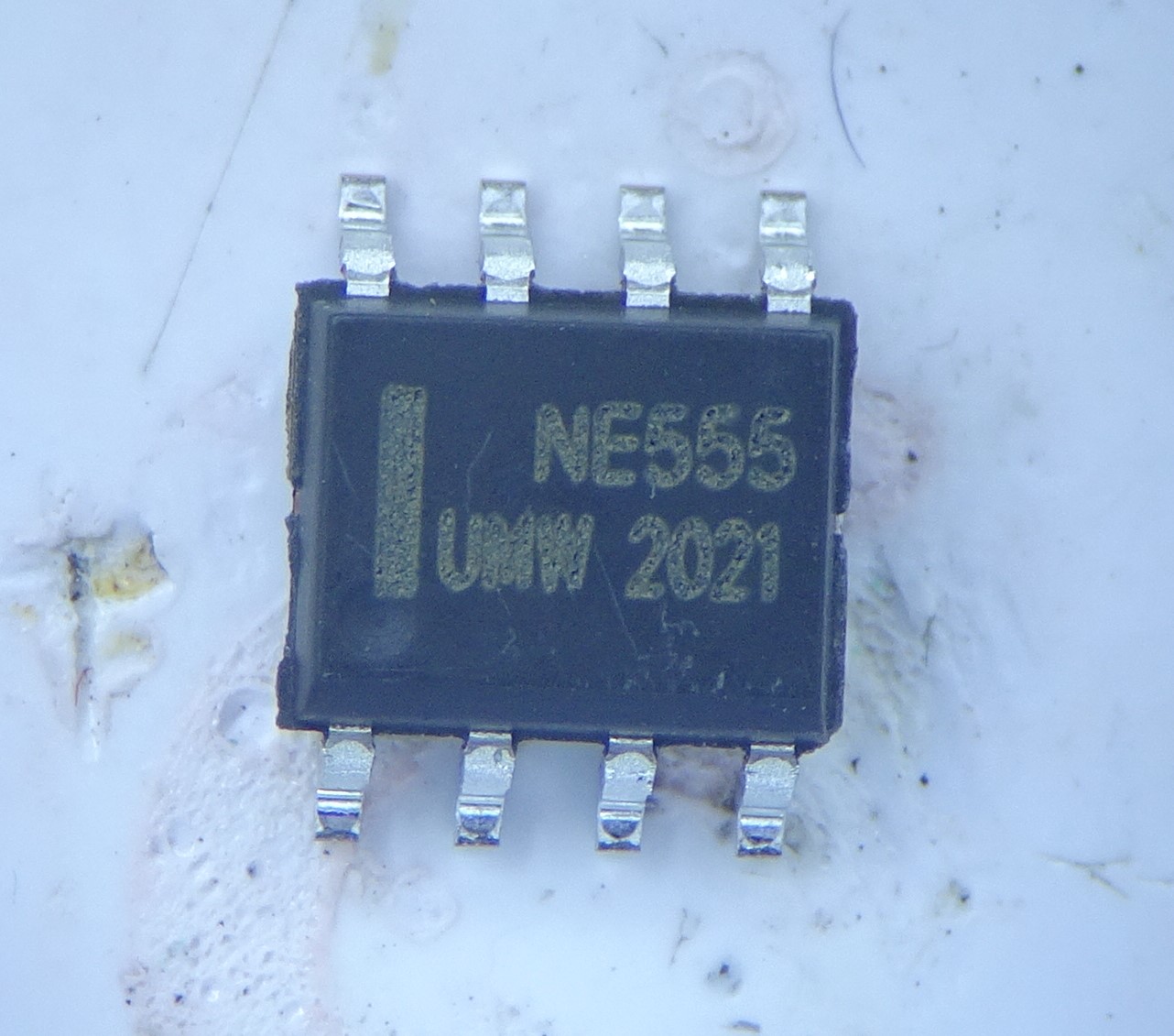
Another Chinese manufacturer with the NE555 in its portfolio is UMW. Its datasheet is again a direct copy of TI’s.
Inside it’s yet again a new design. The manufacturing process looks similar to the two HGsemi chips’, with the square PNP emitters with round contacts. The diffusions are also hard to distinguish, but in this layout the three 5k resistors are easy to find between the Discharge and Threshold pins.
For some reason I really don’t like this layout. It’s hard to quantify “ugly”, but the way many tracks are routed and the way the transistors appear to have been dumped at random makes it unpleasant to look at.
Again, the circuit is the same as TI’s and HGsemi’s. But the layout just makes my eyes hurt: for example, in Q1 and Q2 the base and emitter are arranged horizontally, while in Q3 and Q4 they’re arranged vertically. Simply rotating Q1-Q2 by 90 degrees would make the metal routing much cleaner. Also, note how the closest P-sub contact to Q10 is the emitter of Q8! The collector current of Q10 will have to flow quite a distance through the substrate.
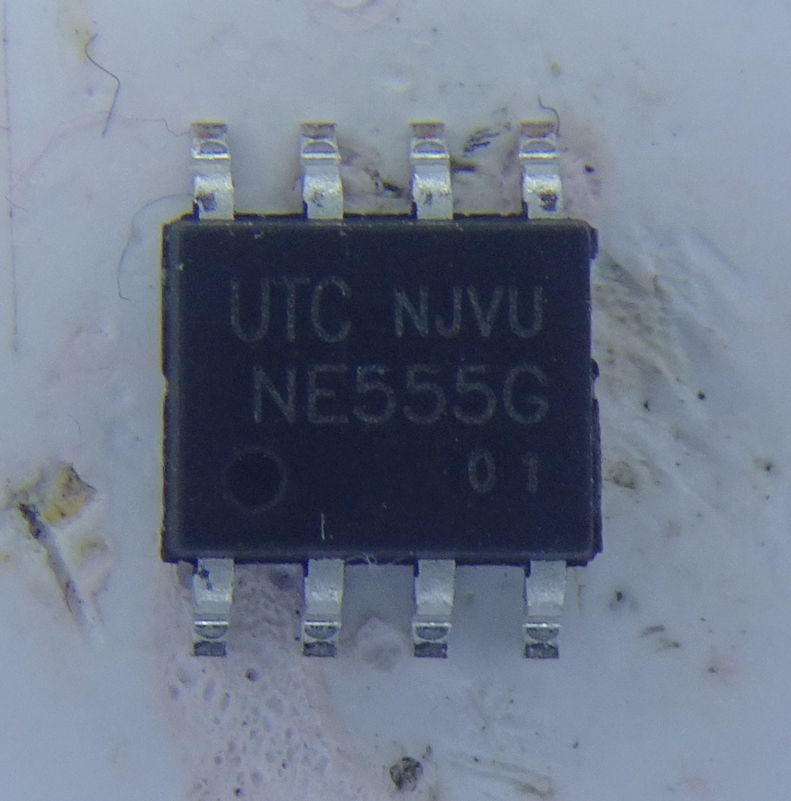
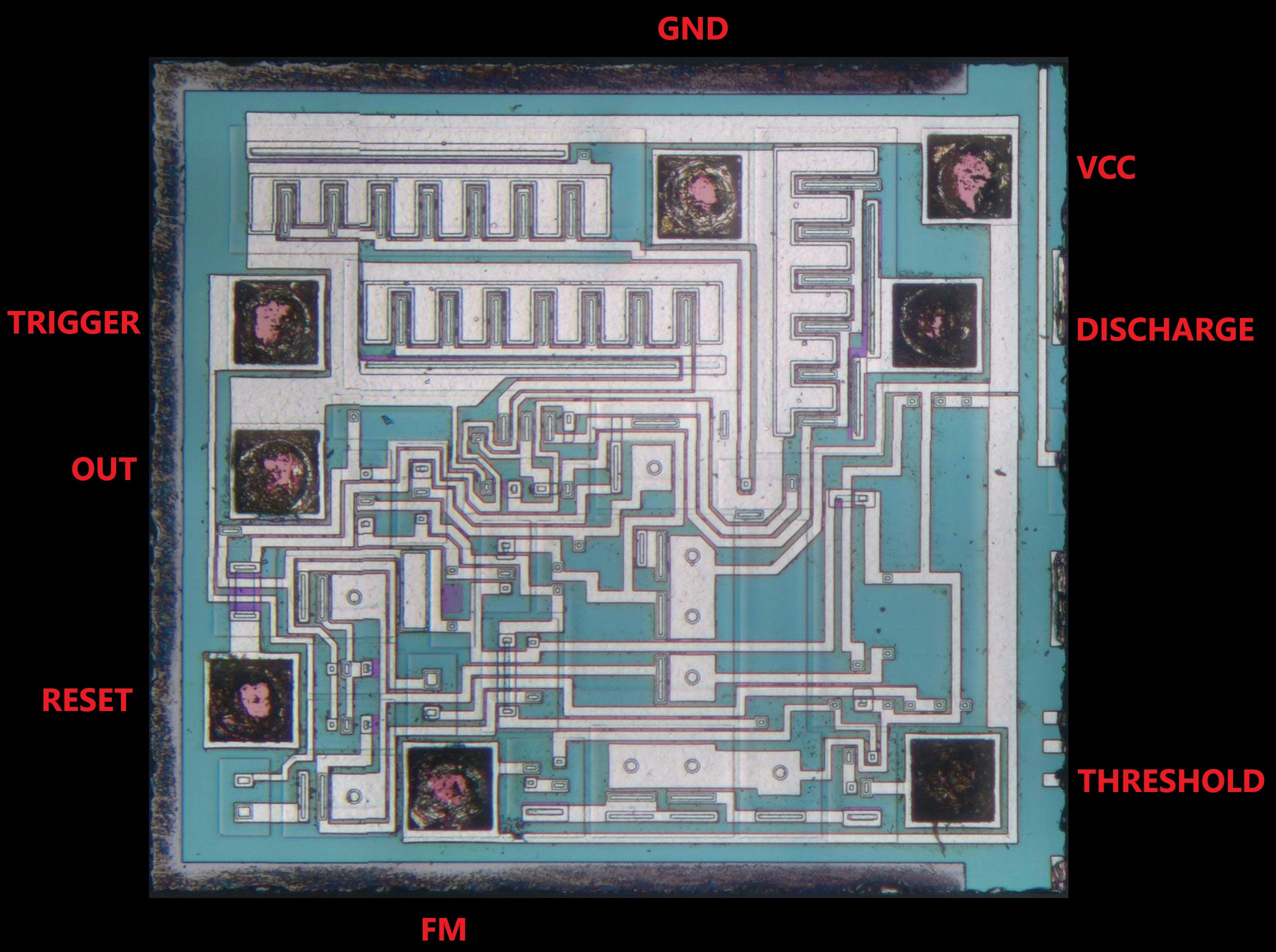
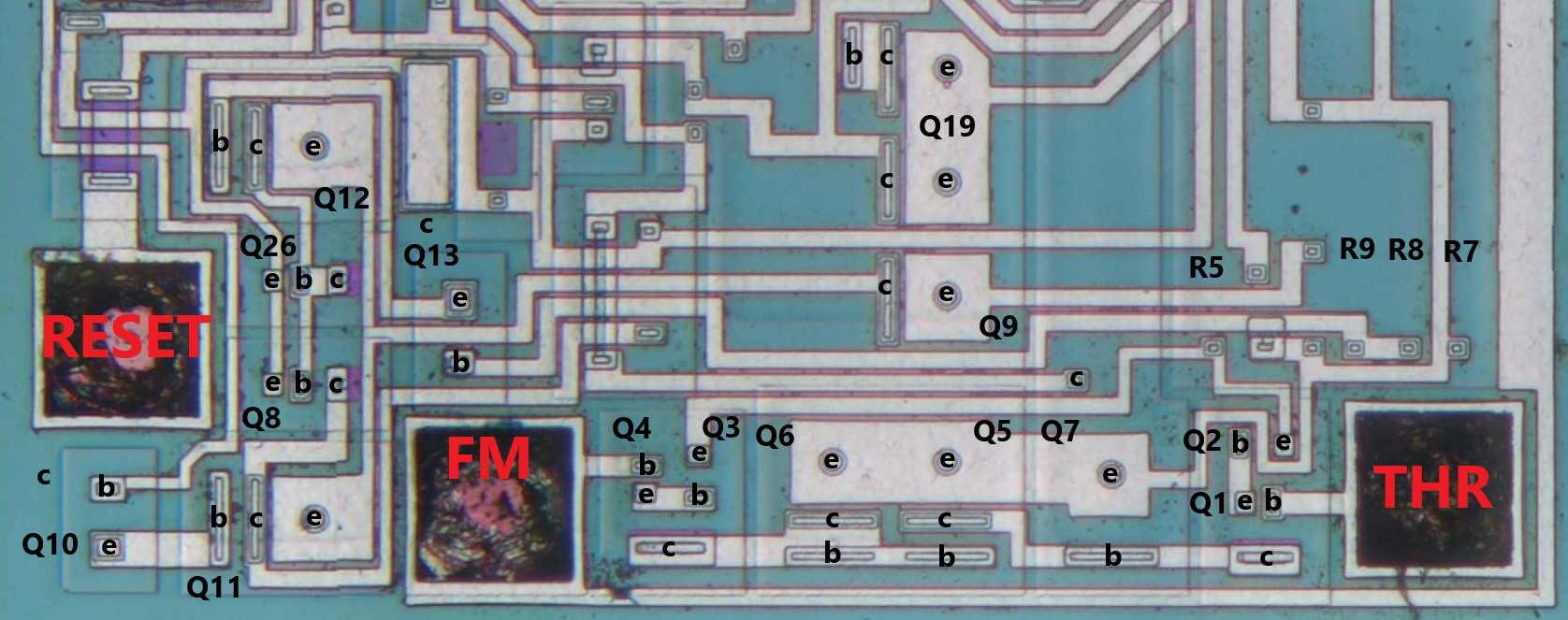
The last 555 timer for today is UTC’s NE555G. UTC is a Taiwanese company with its own fabs, and has a reasonably wide portfolio of simple analog and digital ICs.
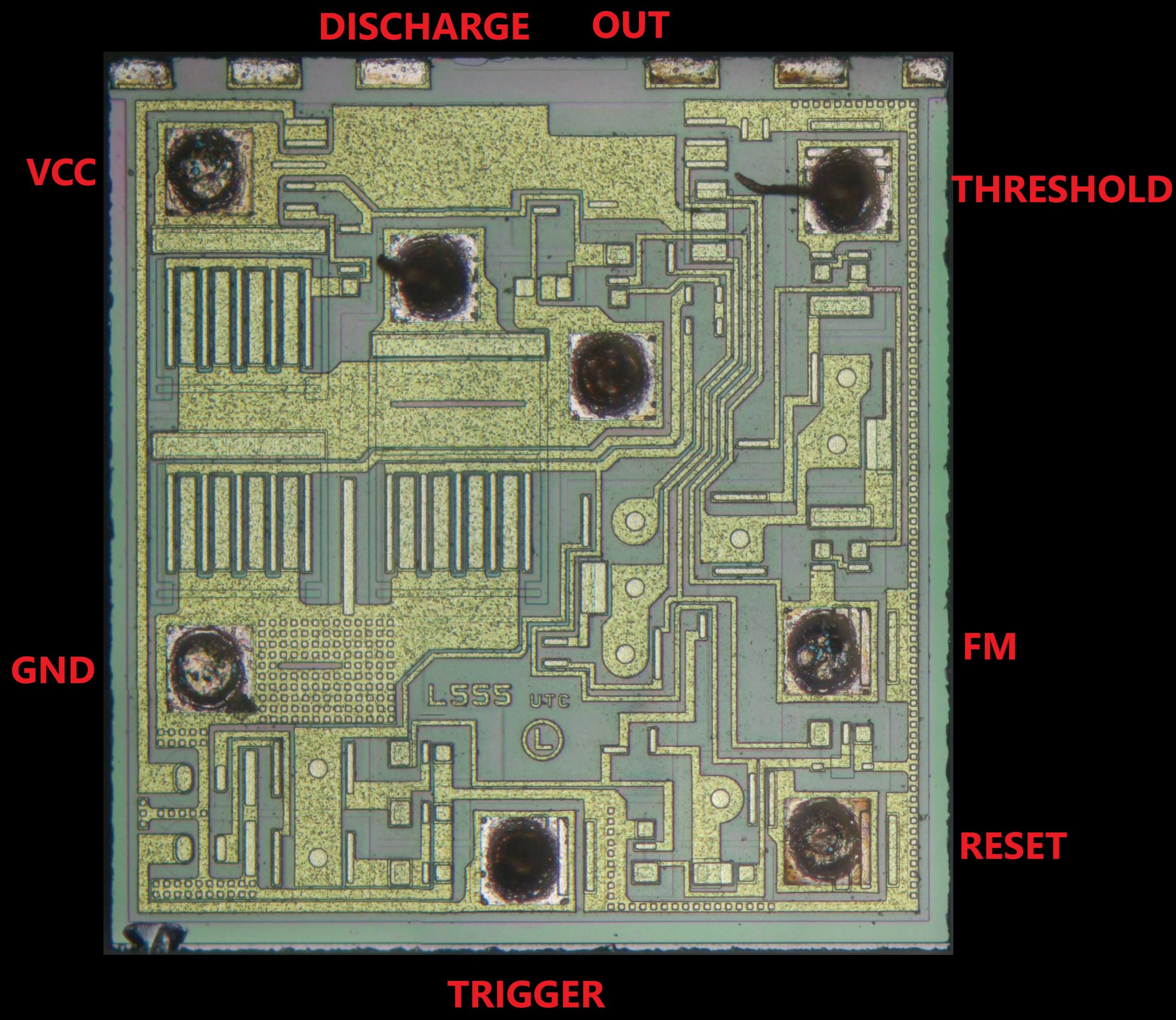
UTC did include their company name and an identifier “L555”. I’m not sure what the circled “L” means though. The layout looks well-organized, and once again we find nice round PNP emitters. The three 5k resistors are at the top, roughly between the VCC and Threshold pads.
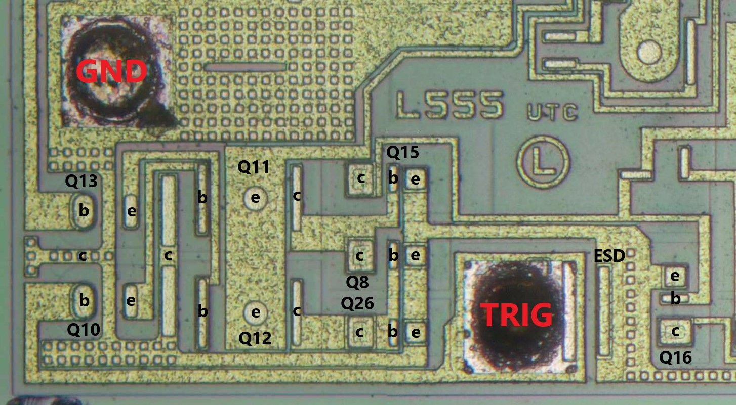
Unlike UMW’s, I really like this layout: it shows that someone knew what they were doing and put in the effort to optimize everything as much as possible. Transistors that need to be matched are laid out symmetrically and arranged to minimize wiring. Note also how there are lots of substrate contacts around vertical PNPs Q10 and Q13, to prevent substrate currents. There’s a nice bar with thick substrate contacts between Q10-Q13 and Q11-Q12 to ensure that no current flows below the surface between these two transistor groups. The circuit is yet again the TI variant. Also note that there are ESD clamps next to the bond pads.
This has become quite a long article, but I like the way you can see how different manufacturers produced the same design in so many different ways. It’s also interesting to see how all “modern” versions of the chip contain the same modifications compared to the original. I suspect that chips from the ’70s and ’80s will be closer to the original design, like the Thomson chip. I’ll try to find some older chips in order to test this hypothesis 🙂
Very interesting and nice work.
Is there a plug and play replacement for the SOP8 UTC NE555G? Somebody please, I need some help.
What they call SOP is most likely almost identical to what other manufacturers call SOIC, so you should be able to use any of the chips shown on this page.
Can you recommend one from this site? Can’t make up my mind reading about all the different makers. What about the LM555CM? Thanks.
It’s a very simple and cheap chip, so it really doesn’t matter which one you use. Having said that, I would still go for one of the large, well-known manufacturers like TI or ST. They are readily available anywhere, and with these companies you know that they have proper quality control in place. With small, unknown manufacturers whose datasheets are sometimes copied word-for-word from TI or ST you can’t be so sure.
I first started using the 555 in about 1976 while still in college for a sign flasher. I started working for Signetics in 1990. Hans Camenzind’s comment on the LM10, introduced a couple years earlier (in 1978) was that it was “overdesigned.” He would have been one of the few on the planet qualified to make that statement. (Signetics business cards were embossed with the 555 metalization pattern. Hans’ was printed longitudinally instead of laterally.)
ps: I started at Signetics in 1980.
Hi David, that’s interesting to hear! Did you work directly with Hans Camenzind at the time? I’ll definitely add the LM10 to my list, because it looks like I haven’t dissected any of Bob Widlar’s designs yet.