Texas Instruments has a nice selection of motor driver ICs. Where in the old days you’d often have to make your own H-bridge out of discrete transistors, figure out how to drive their gates, and then generate the right signals to spin up, reverse, brake or coast your motor, nowadays you can get all these functions integrated into a single chip. Today we’ll look at the DRV8876, which is a rather small chip that can nevertheless dump up to 3.5 A into a motor’s windings.
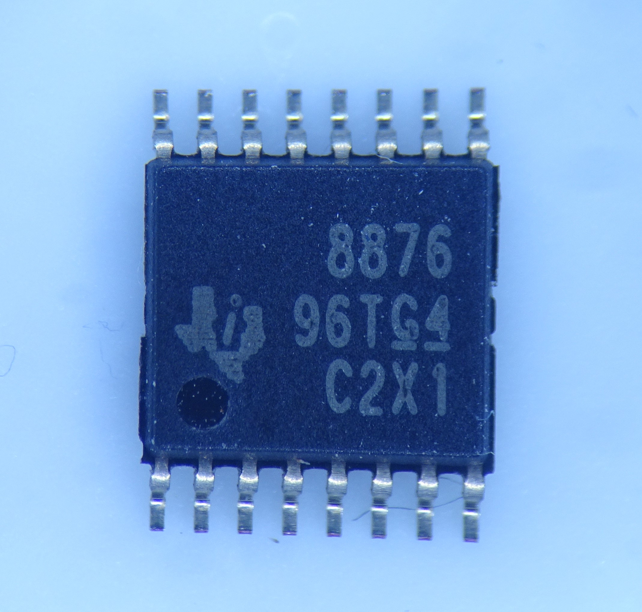
This chip is housed inside a tiny HTSSOP package, measuring just 5.0 mm by 4.4 mm. On the front we find the TI logo, the part number and some production codes. Inside, it’s got a full H-bridge as well as a current sensor to stop your motor windings from going up in smoke when the motor stalls. It’s also got a charge pump to generate the high voltage needed to turn on the high-side NMOS transistors. The chip can work at supply voltages up to 37 V.
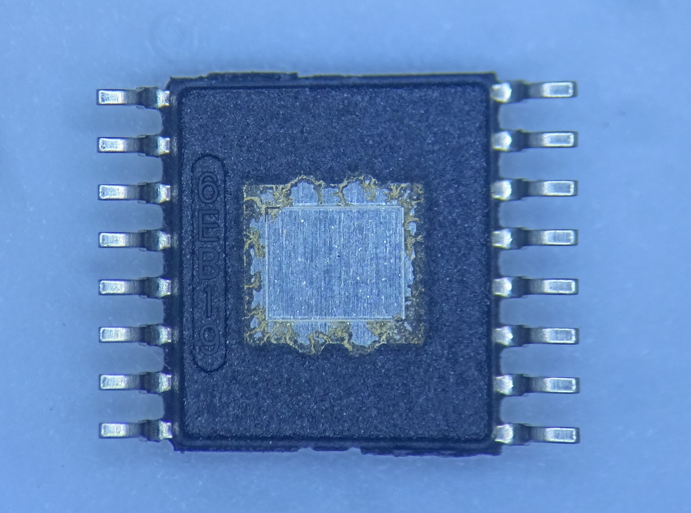
The back of the chip has some other production code as well as an exposed thermal pad. This is meant to be soldered directly onto your PCB and facilitates the transfer of heat from the chip to the board. It’s interesting to see how the plastic moulding compound seems to have crept a bit onto the edges of the thermal pad; that almost looks like it shouldn’t be that way.
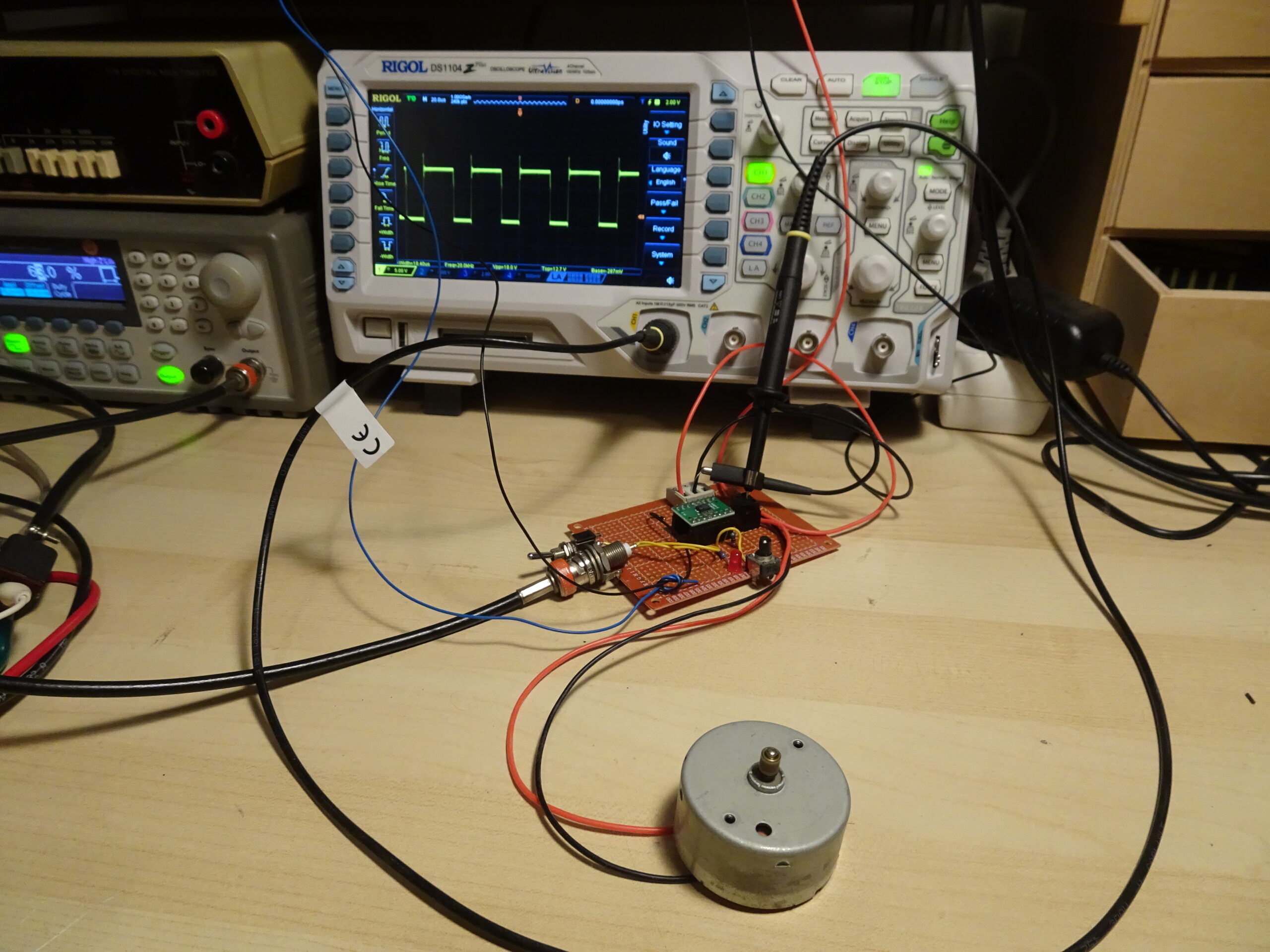
I soldered together a simple test board to try out the chip’s functionality. The function generator on the left outputs a PWM signal that the DRV8876 then uses to drive its power transistors. It can also sense the current flowing into the motor and gives a signal when it exceeds a certain (programmable) amount. The duty cycle of the outgoing signal is then automatically reduced to keep the motor current within a safe range.
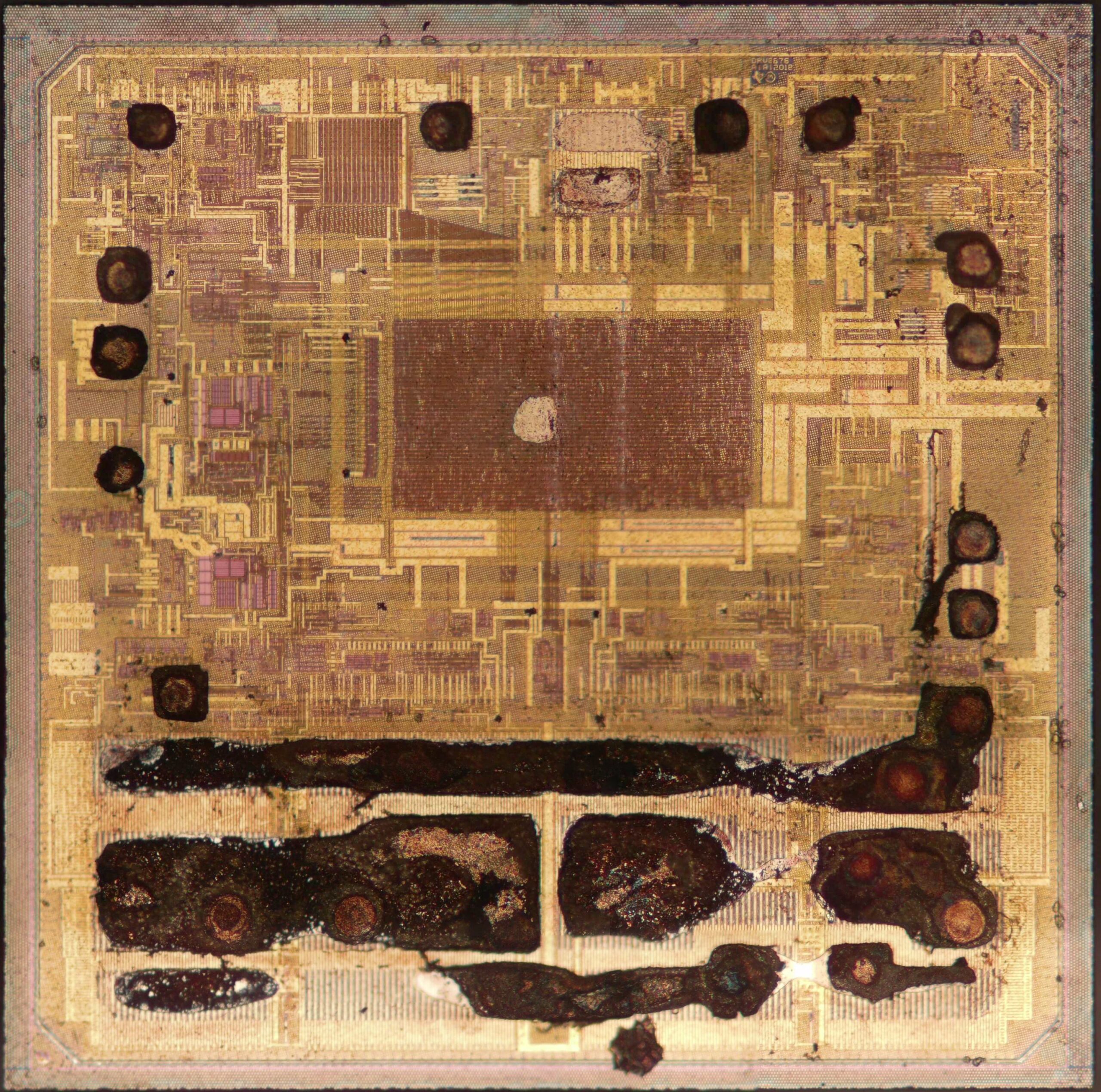
When we take a look inside the chip, several things stand out. First, we can see that this chip uses a very thick copper top metal layer. At the lower end we see the remains of two narrow horizontal strips, which are the H-bridge’s supply and ground lines, and two thicker strips which form the two output pins. Much of the copper was stripped away during the chemical etching process, leaving these copper smudges behind.
Second, we can tell that the bond wires were also made of copper. The wires themselves are gone, and studs remain where they were bonded to the chip. TI was one of the first manufacturers to apply copper wire bonding in production quantities; gold has always been the standard material because it was easy to work with, despite its much higher cost compared to copper. Advances in wire bonding technology have enabled the use of copper, which is not only cheaper but also has a significantly lower resistivity than gold.
Third, this chip’s design is way more complicated than I thought it would be! I would have expected the large power transistors and their slightly smaller drivers, plus a few logic gates and some small analog circuits (comparators mostly), but this chip has a significant amount of digital logic (the brown rectangle in the centre) and huge amounts of other stuff scattered across the die.
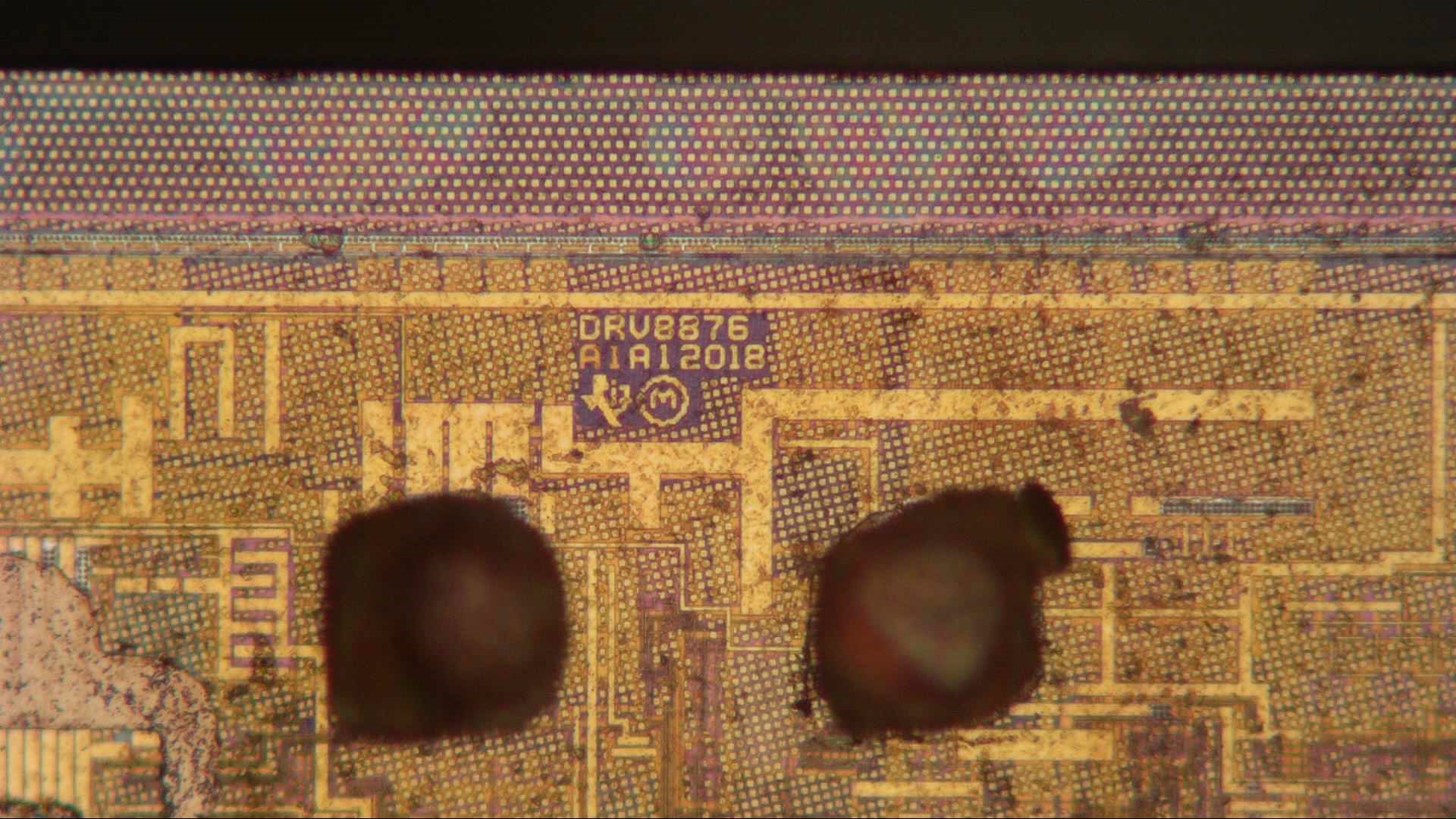
Zooming in a bit, we find the chip’s identifier as well as a 2018 copyright date. The grid of little squares that covers the chip is a grid of dummy structures, which are necessary to ensure proper smoothness and constant etch rates across the whole chip. These are usually seen on technologies measuring 130 nm and below.

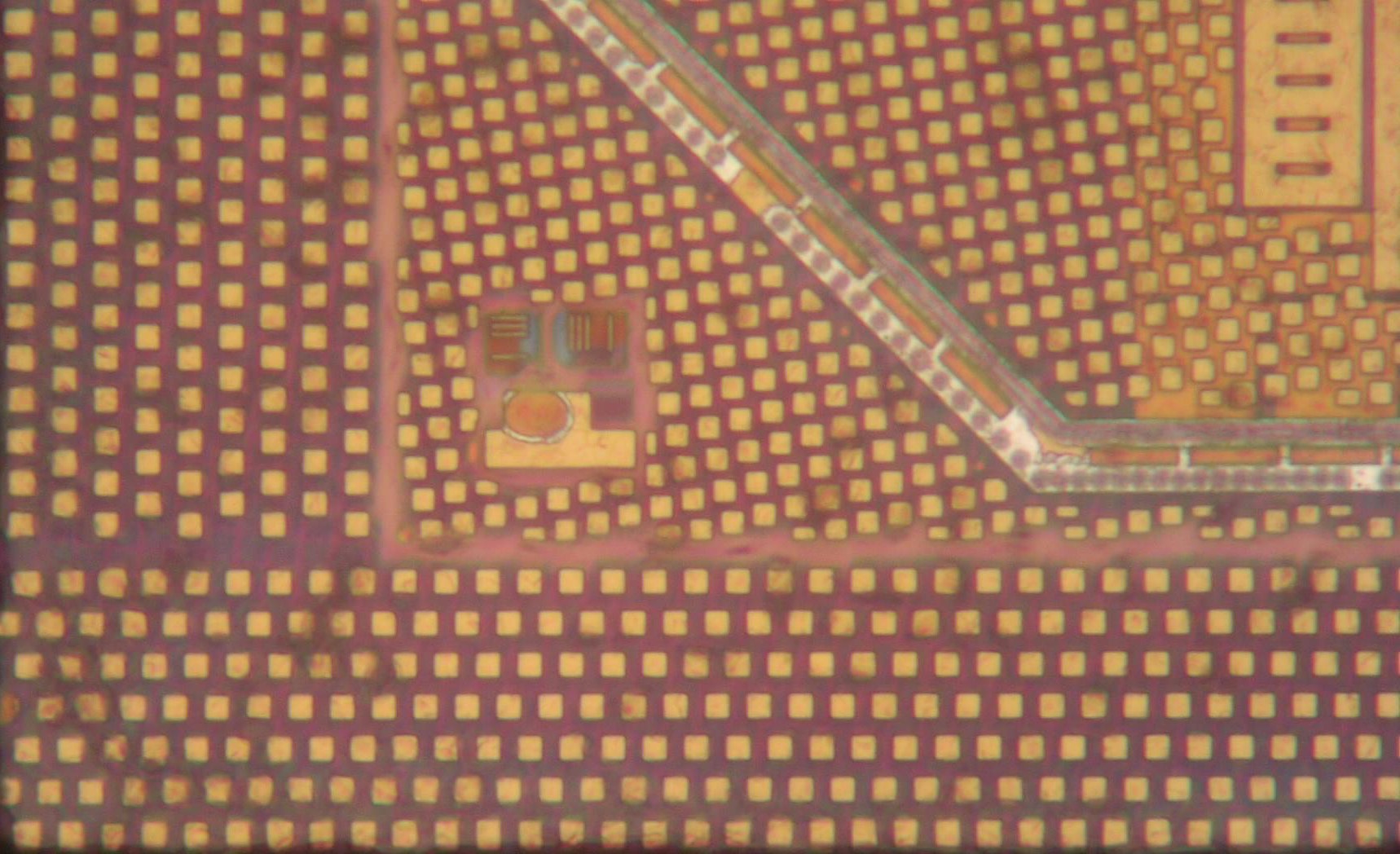
Here’s what looks like a piece of analog circuitry. The pink rectangles could be capacitors or large transistors. Note how the dummies have been omitted on top of these devices.
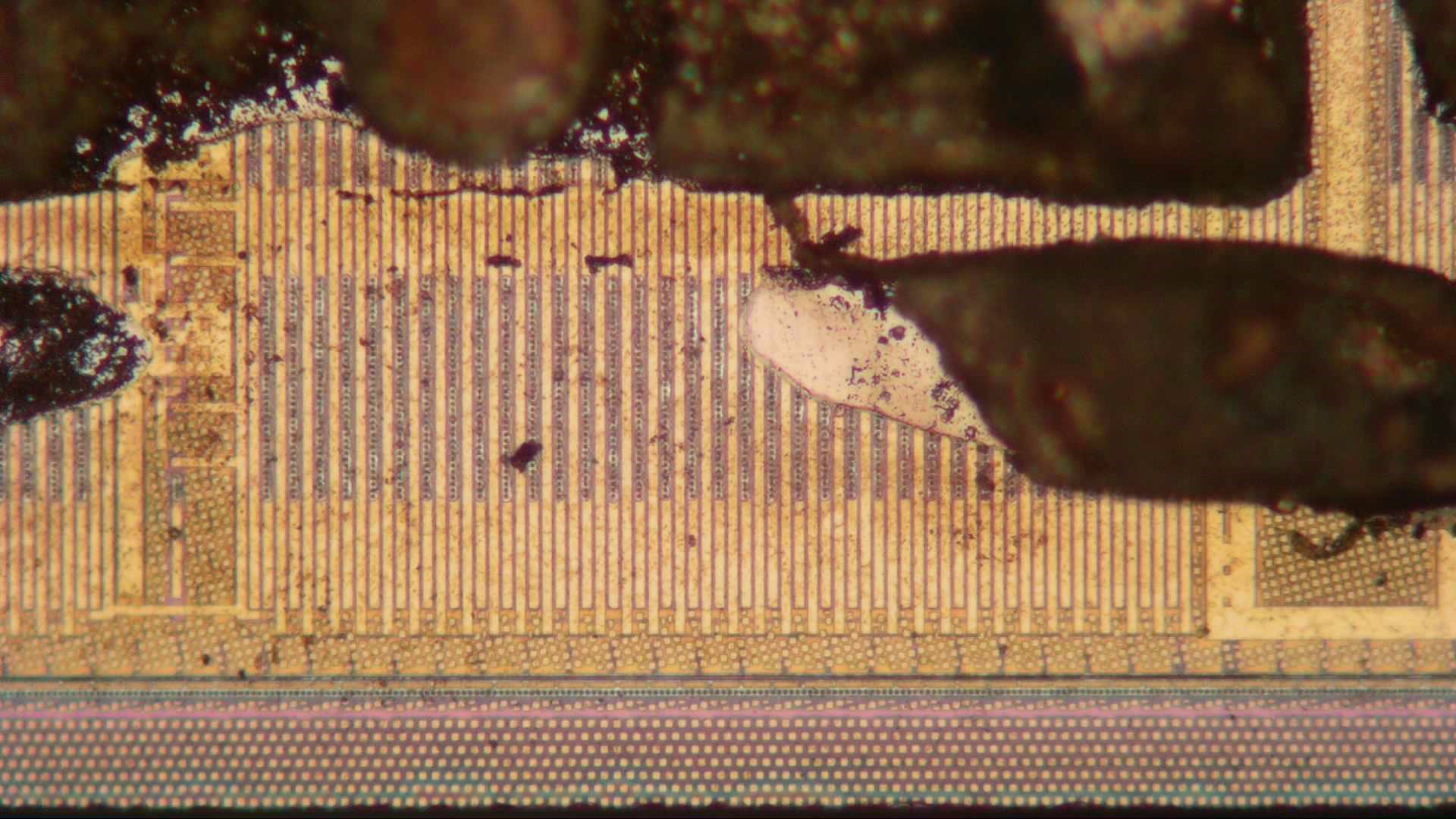
If we look at the power transistors, we find a very fine-grained finger structure. The source and drain terminals alternate along the width of the transistor. Only one set is connected to the metal top layer using a set of vertical contacts.
In the bottom-left corner, among a sea of dummies, is this feature that looks like an alignment marker of some sort.
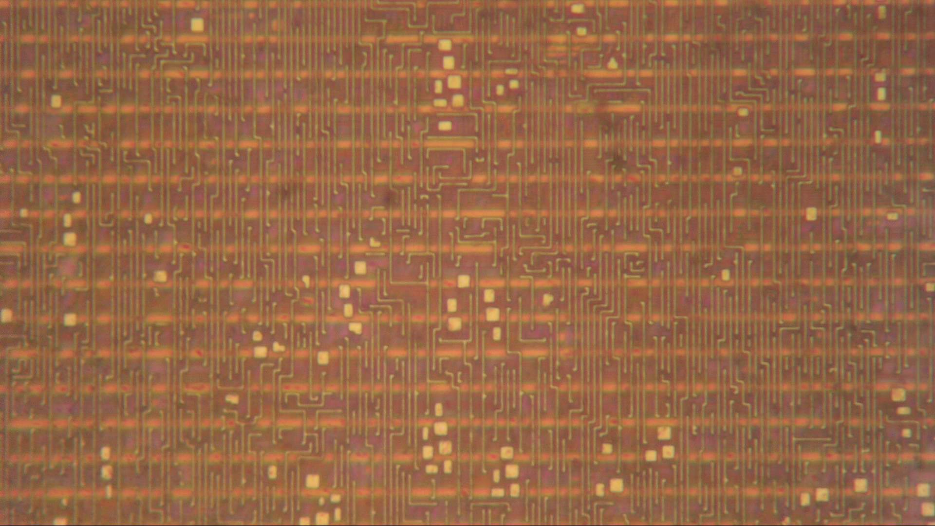
When we look at the digital area in the middle of the die, we can clearly see the routing on the top metal layer. A few layers down we see the logic cells as dark horizontal strips. Note how the top metal layer is quite dense, but still requires dummies here and there (the bright squares). As I mentioned before, the total amount of logic looks rather large for such a simple chip: the basic functionality seems to me to be just some AND-ing and OR-ing of input signals, and handling a few fault conditions (overcurrent, overtemperature, undervoltage etc). The logic here looks complicated enough for a simple microcontroller. Maybe this chip performs some clever auto-calibration when it powers up? Maybe it’s just for automated production testing in the factory? Who knows, but in any case implementing lots of digital is easy in an advanced process like this.