Back in 2016, TI introduced a line of what they called “nanopower op amps”. Where older op amps like the 741 use around 2 mA, and more modern ones might reduce that to perhaps 100 uA or so, TI’s ultra-low power devices consume just a few hundred nA. This enables the design of things like smoke alarms and temperature monitors that can work for a decade on a single battery charge.
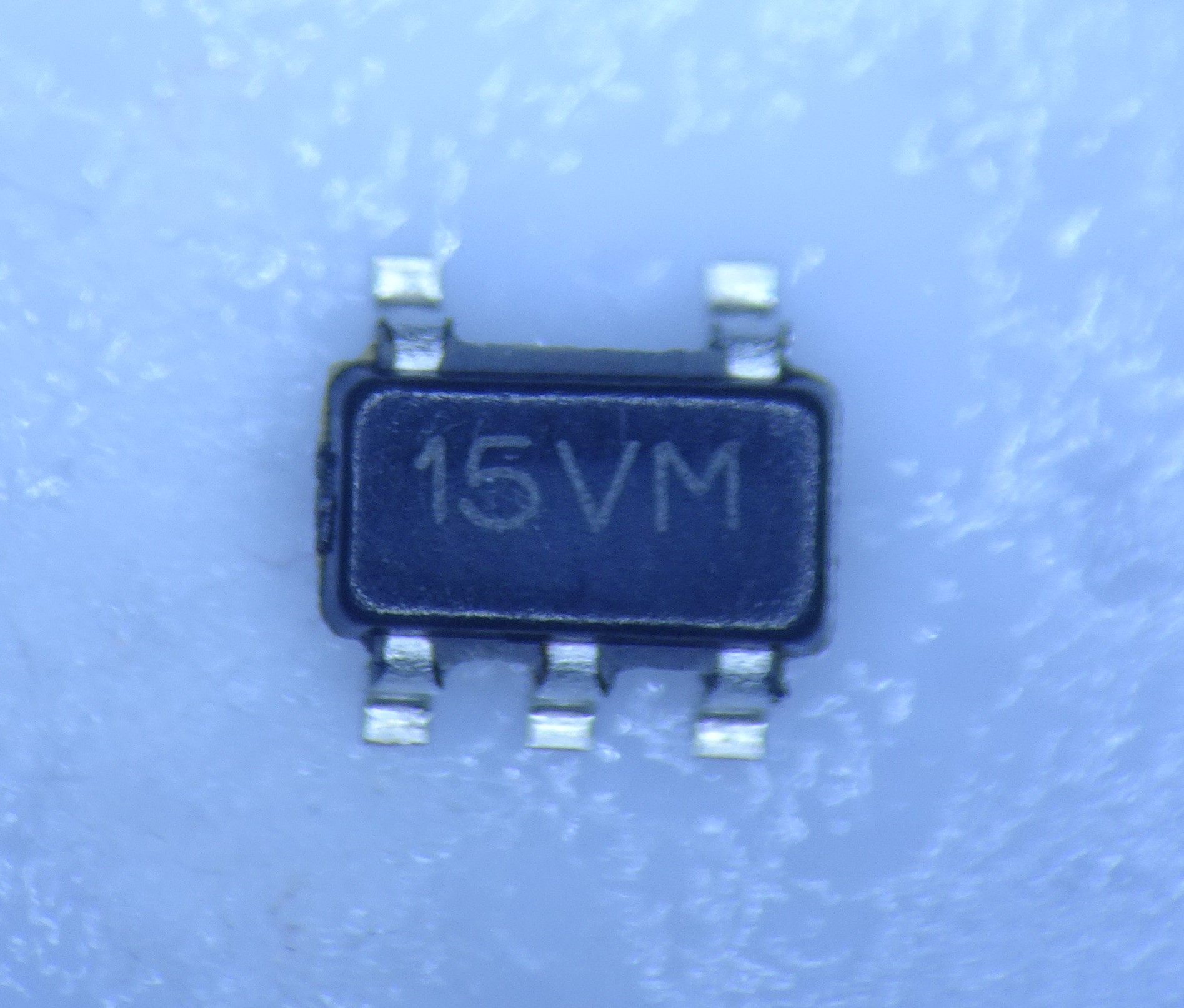
This is the LPV801, a single channel op amp that uses just 450 nA. It’s not very fast: with just 8 kHz of unity-gain bandwidth it’s useless for audio, but ideal for slow-moving things like temperature sensors. A dual version (LPV802) is also available, as are single and dual versions with reduced offset voltage (the ‘811 and ‘812 respectively).
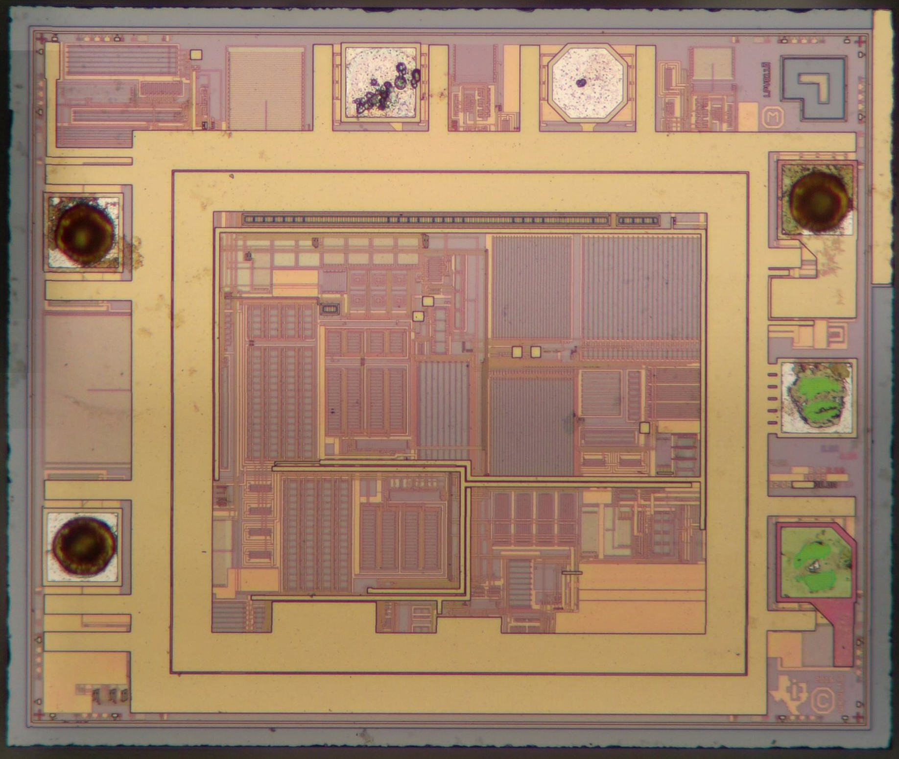
Inside we find this neat little design. Five bond pads are bonded to the five pins on the package; two additional ones on the top row are used for testing. In the top-right corner is an L-shaped alignment marker, which is used during laser trimming.
This chip is laser trimmed to ensure its performance is within spec. The long horizontal bar we see here, with little yellow and black vertical lines inside, is a row of laser fuses. When the chip is manufactured, each of these positions contains a metal wire that connects two pieces of circuit together. The performance of the chip is measured, and the metal wires are zapped with a laser to burn away the wires in specific places.
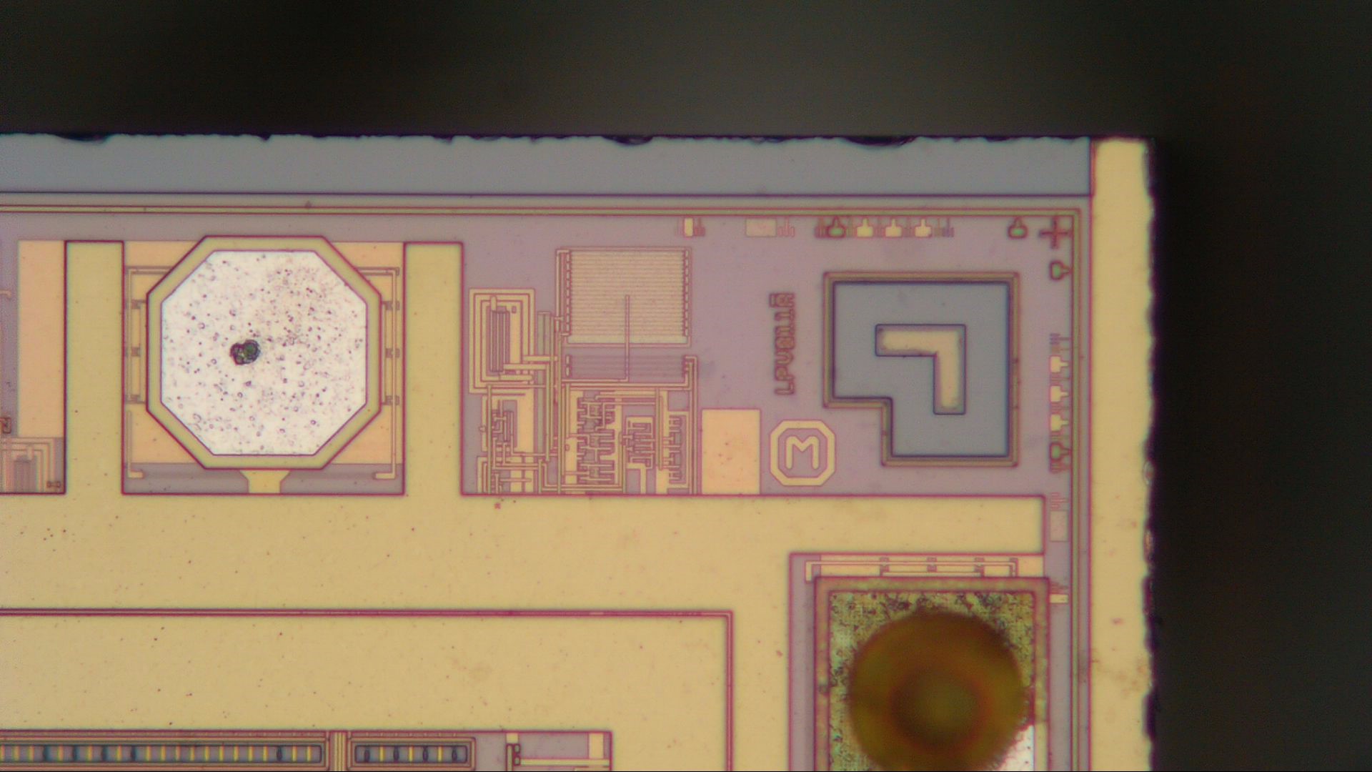
The L-target is used to align the laser to the chip. Next to it we find an identifier LPV801A, with the “A” meaning that this is the first revision of the chip. Some small circuits and various process control shapes are also present in this corner.
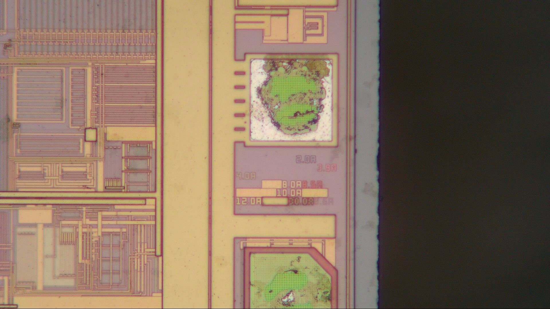
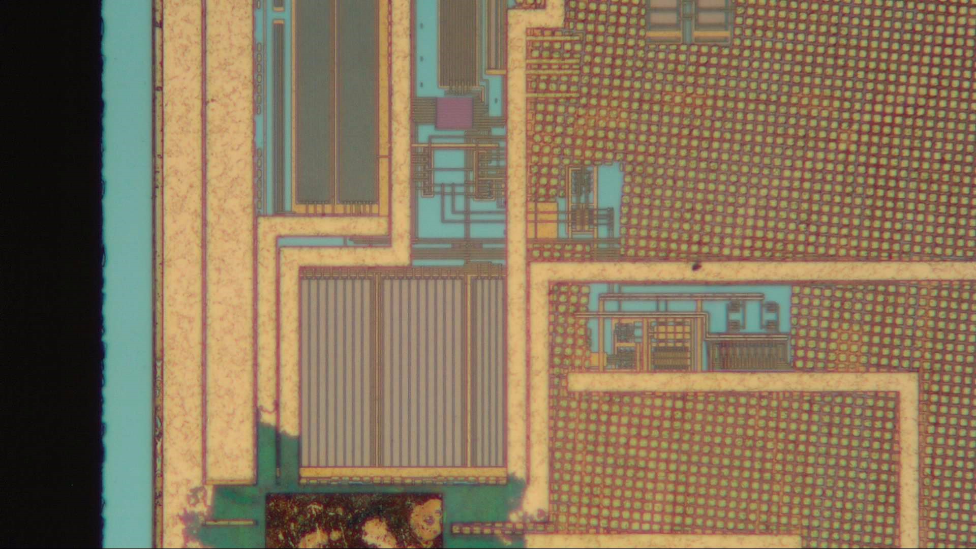
Below the VSS pad we find layer identifiers. All are in revision A as well, meaning that this design was correct from the first tape-out. On the left we see lots of analog circuitry, much of it consisting of long, thin transistors and resistors. These are necessary to achieve the high resistances needed for ultra-low power consumption.
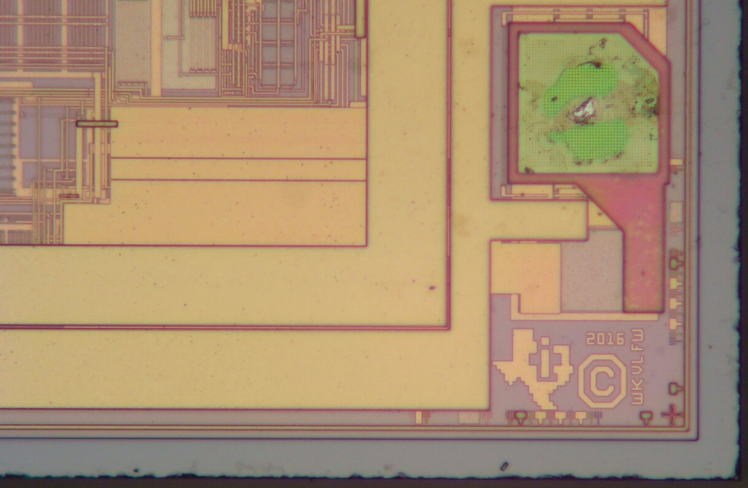
At the bottom-right corner, right below the output pin, we find the TI logo, a 2016 copyright date, as well as the letters WK, VL and FW, which refer to the chip’s main design team. Good job everyone!
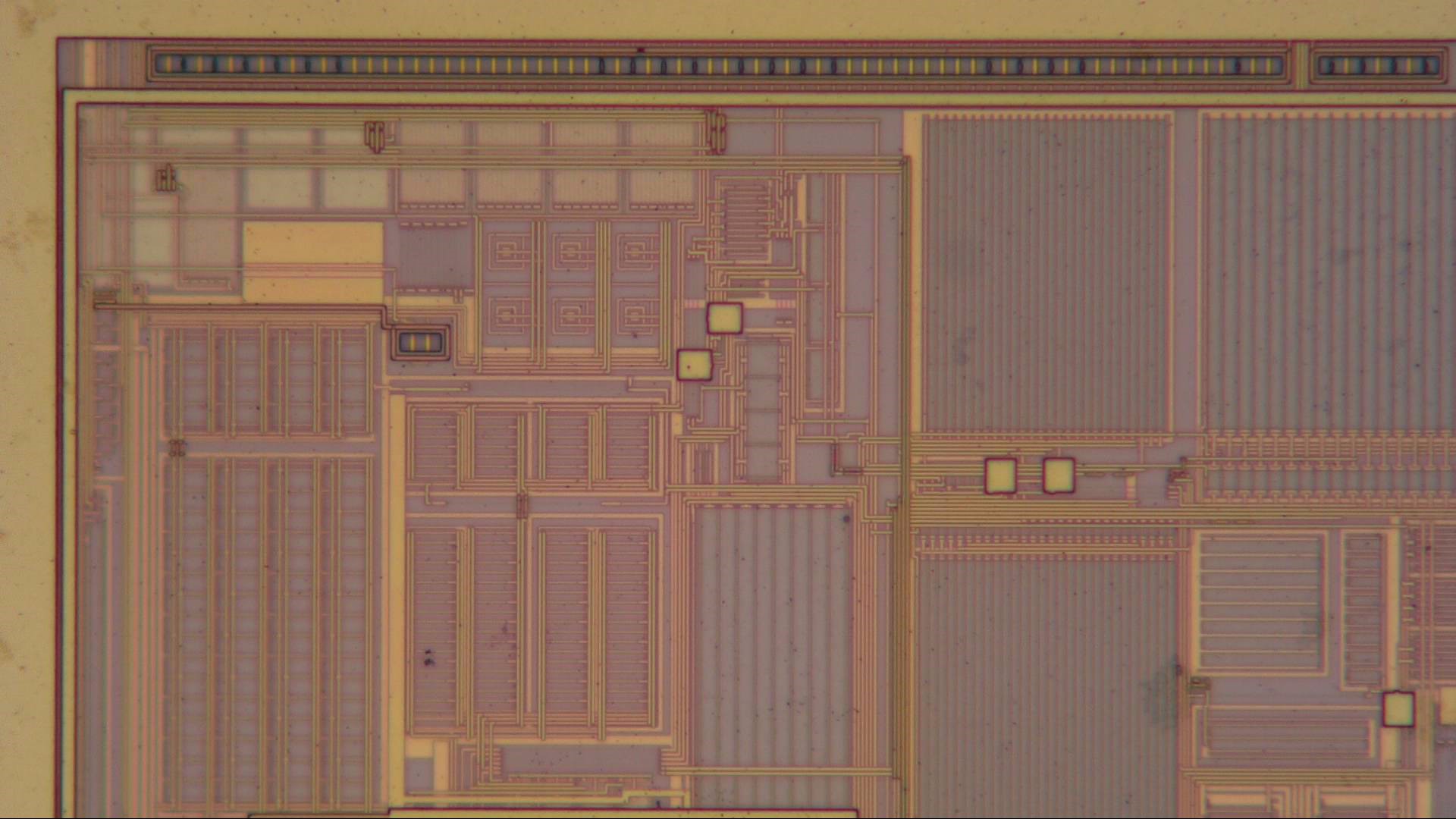
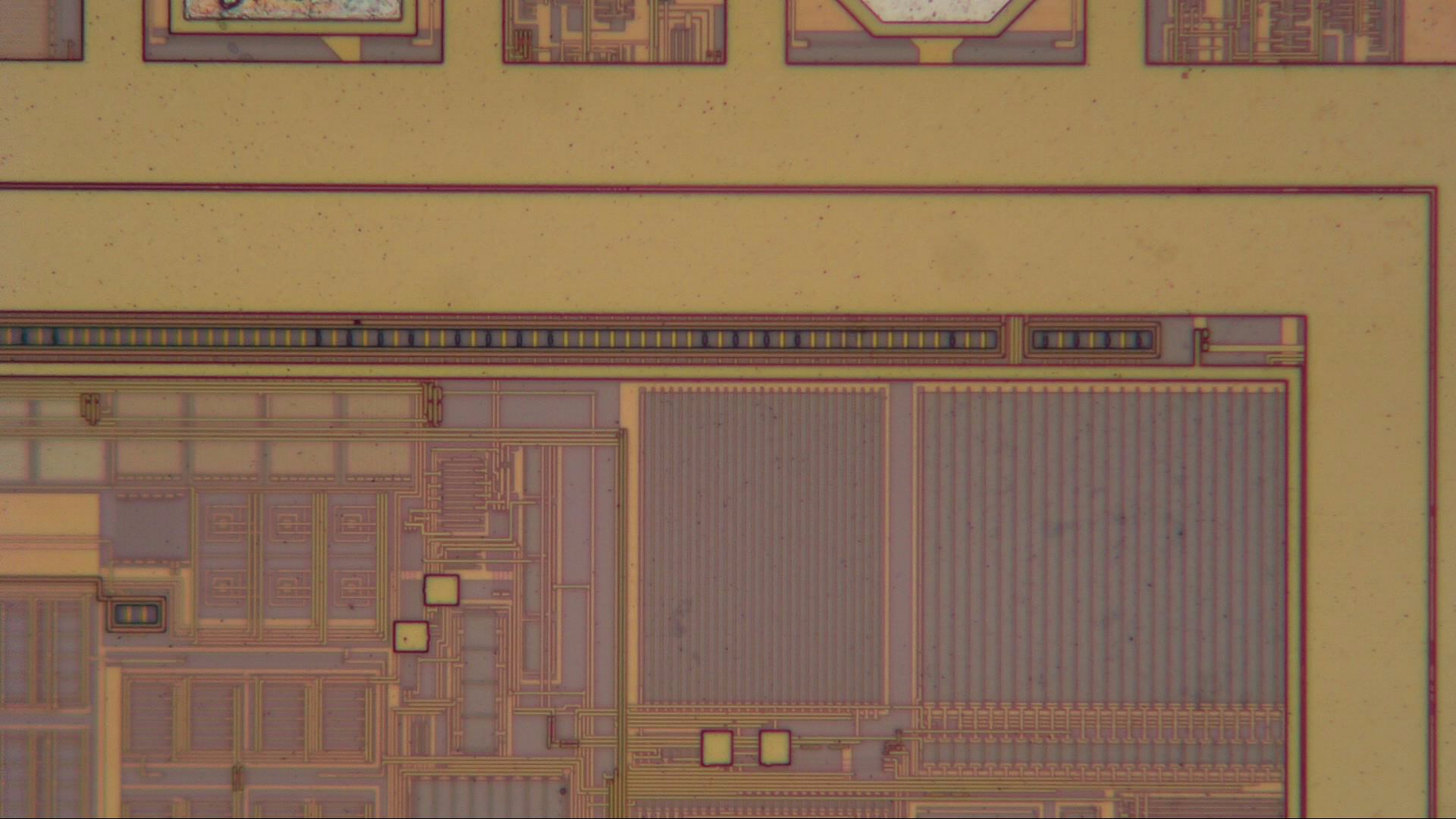
Here’s a closer look at some of the internal circuits. At the top, we see the entire row of laser fuses. Interestingly, there appears to be a little island with two more fuses a little below the main row. Usually you try to put all fuses in one line to speed up the trimming process: the laser then only needs to sweep along the chip once, rather than having to scan multiple places. Perhaps these fuses are directly attached to some sensitive circuit that would not work with the relatively long wires needed to connect to the main fuse row.
Another chip in TI’s nanopower portfolio is the LPV821. It uses slightly more power than the ‘801, but has active offset cancellation that results in an offset voltage of just 10 uV, which is way lower than the ‘801’s 3.5 mV.
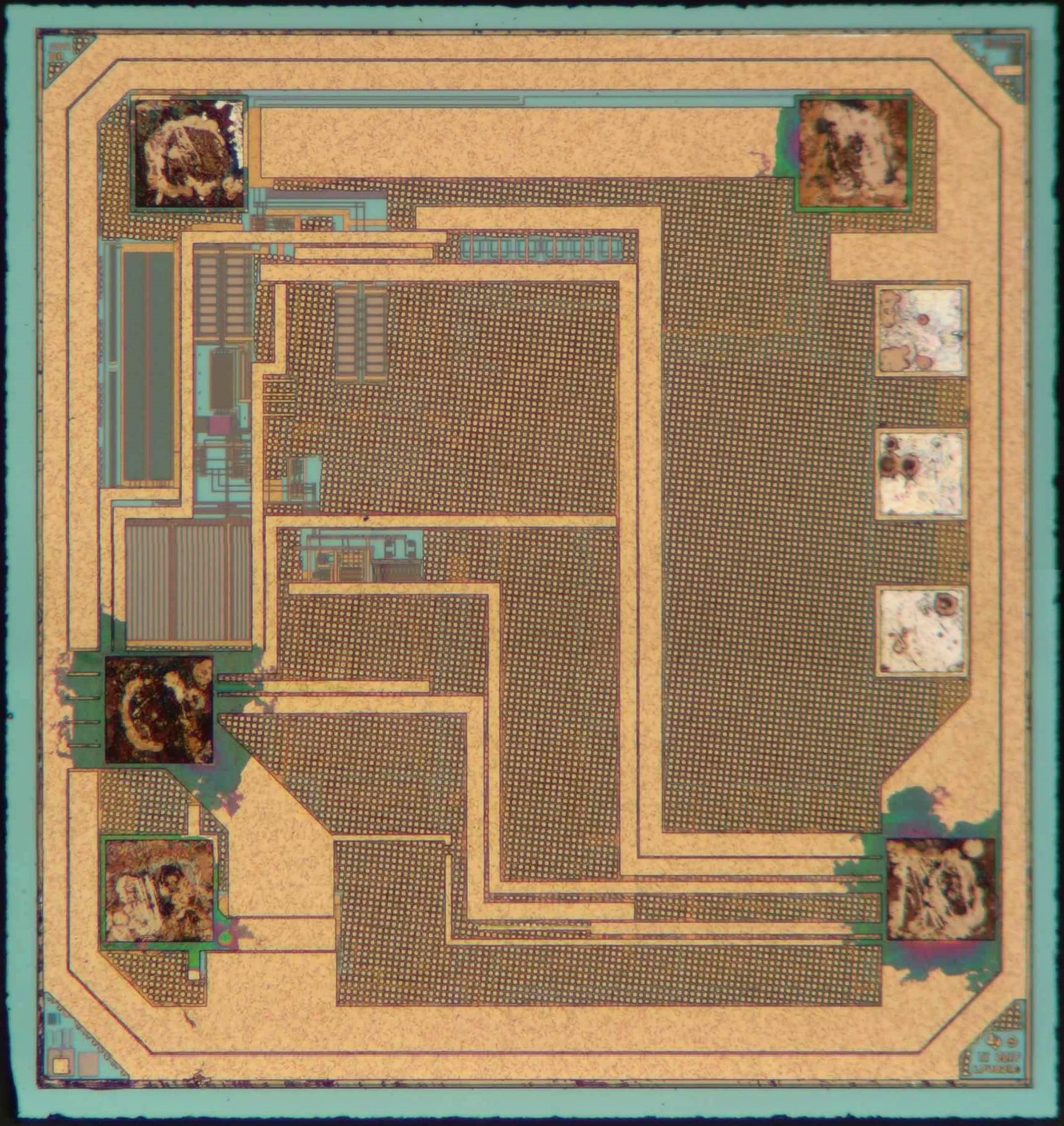
I thought that this would be a derivative of the LPV801, but it isn’t: the LPV821 is produced in an entirely different manufacturing process. Most of the circuitry is obscured by a grid of metal dummies, indicating that this is a more advanced process than used on the ‘801. There are three test pads on the right, but there are no fuses visible. This part could still be trimmed, but it might use something like EEPROM to store its values.
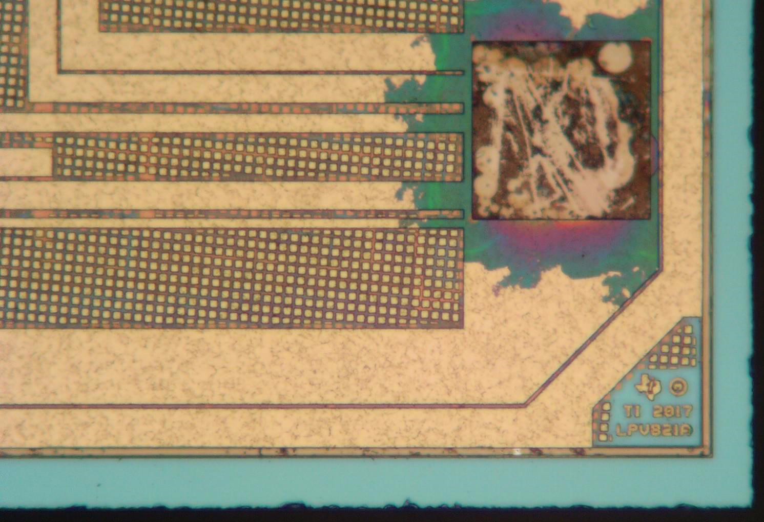
In the corner we find a 2017 copyright date, and an identifier LPV821A, indicating that this chip is also in its first revision.
Some of the circuits that are still visible are these long resistors. Dummies were omitted on top of them to avoid local stress patterns that could degrade the matching properties of these resistors.

Up in this corner we find some revision letters, suggesting that two of the metal layers are in their “B” revision. But unfortunately no initials are found anywhere, so we’re left guessing who exactly made this chip.