LED light bulbs are the most commonly sold type nowadays, especially since incandescent bulbs have been gradually banned from sale starting around 2009. Other low-power types like halogen and compact fluorescent bulbs were also commonly sold until a few years ago, but advances in LED technology, along with a precipitous drop in price, have made LED bulbs the most common type by far.
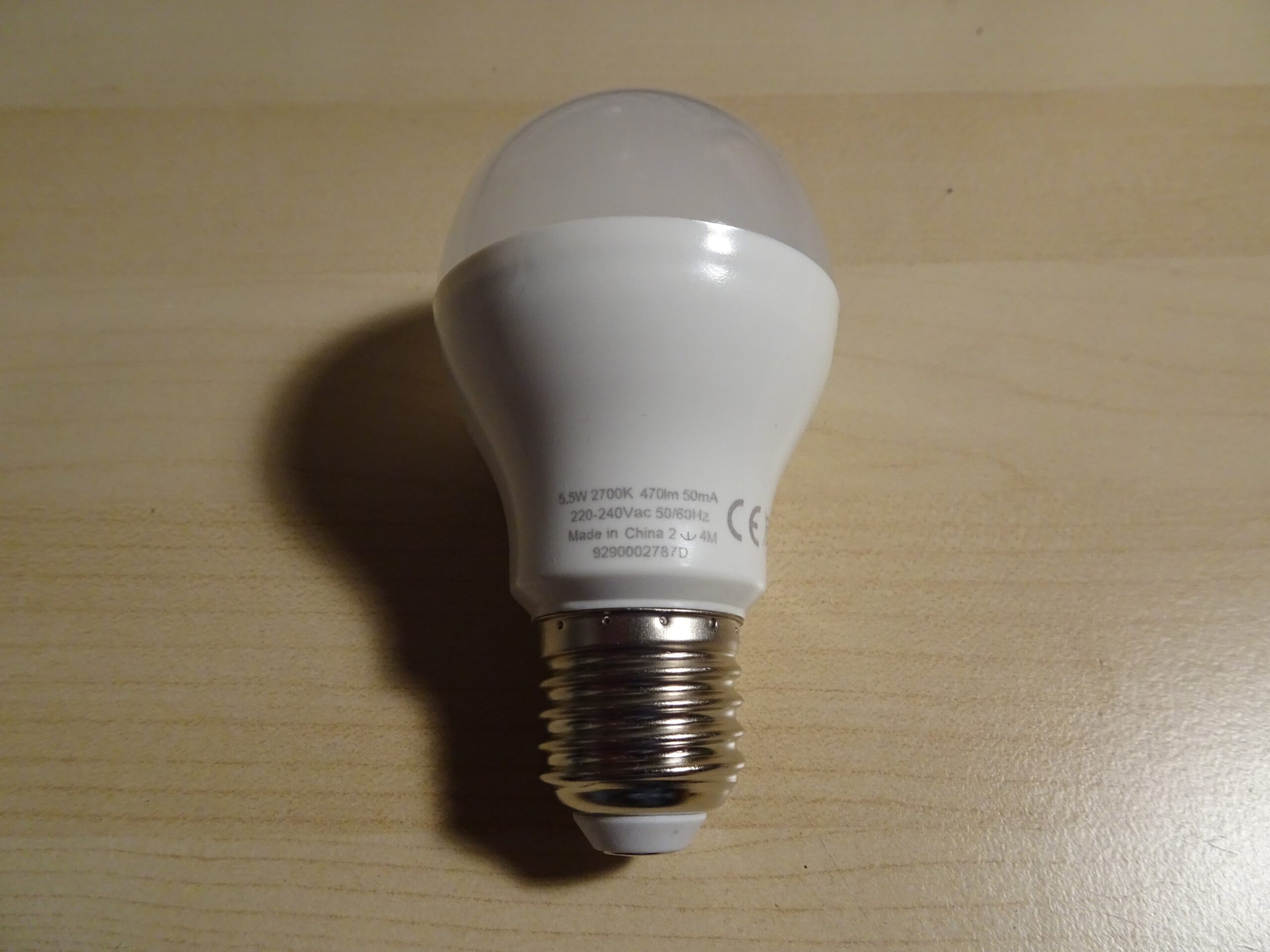
This 5.5 W, 470 lumen bulb had been lighting my home for a couple of years until it burned out a month ago. It was one of the cheapest types sold under the Philips brand; I don’t recall exactly how much I paid for it, but it must have been around eight euros or so. Philips, founded in 1891, is one of the oldest manufacturers of light bulbs, although all lighting products were spun off into a separate company called Signify in 2016.
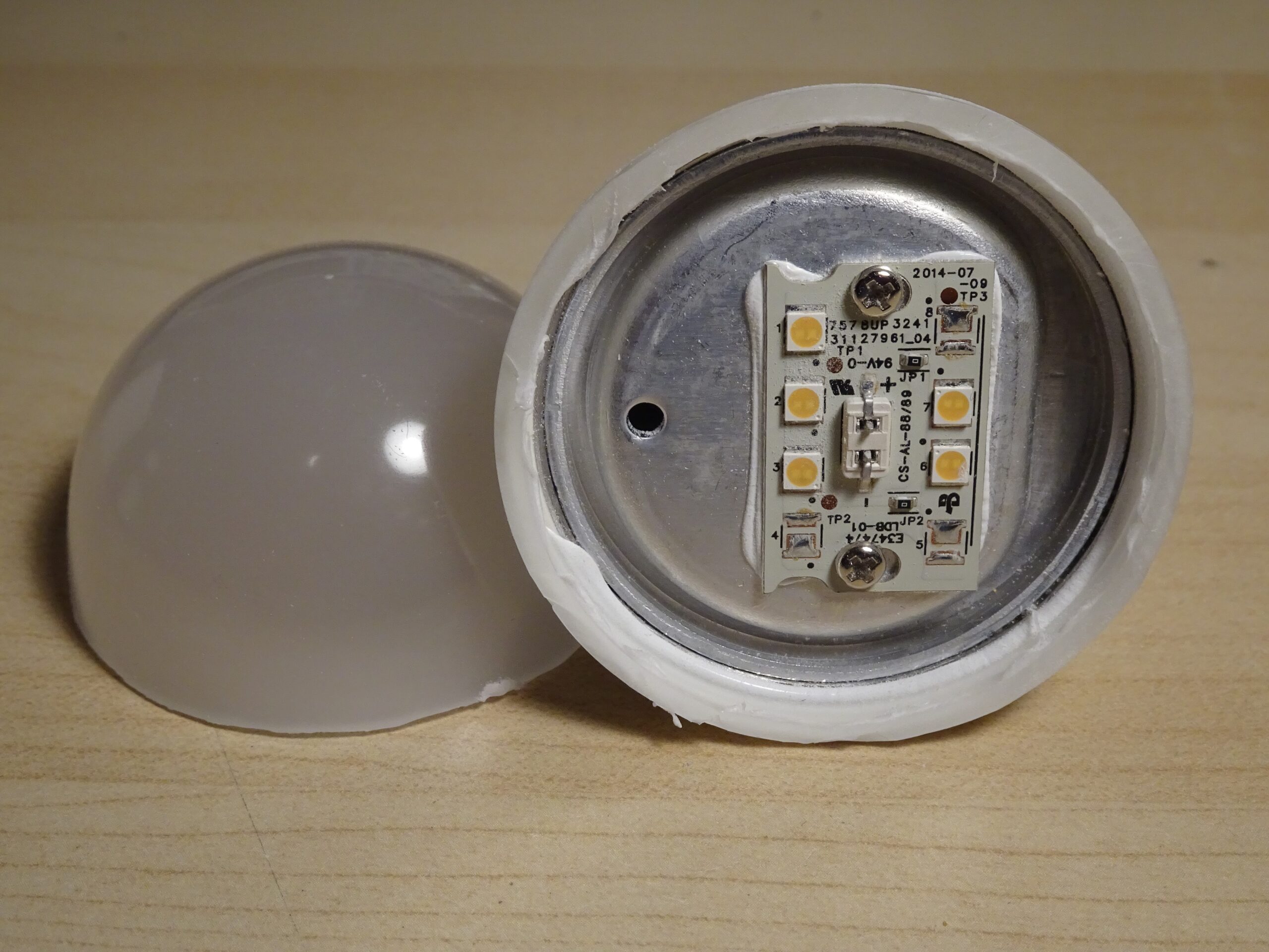
If we cut off the translucent plastic dome, we find a small PCB carrying the LED chips. It’s screwed onto a thick aluminium body that acts as a heat sink. There are five LEDs mounted on the board, but as we can see there’s place for three more. Clearly, the same basic design is also used for a higher wattage version that contains eight LEDs.
All LEDs are connected in series; the three unused ones are bypassed by two zero-ohm resistors (JP1 and JP2). In the middle is a two-pin connector that supplies power from a regulator PCB in the base of the bulb.
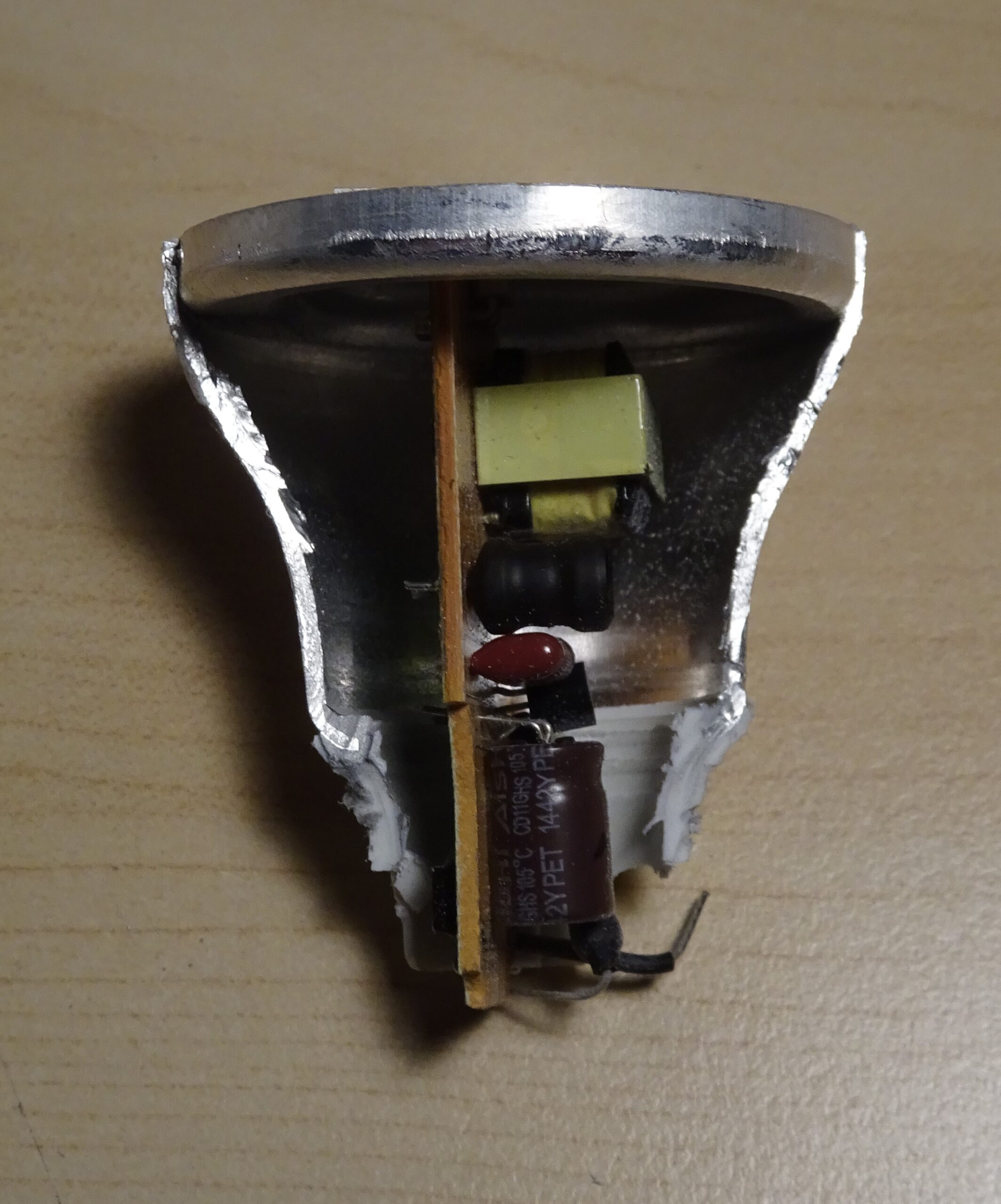
That PCB is mounted vertically like this. Two wires come out of the PCB, connecting to the screw thread and the tip. These supply the 230 V AC mains, which is then converted into about 20 V DC. We can see a large electrolytic capacitor, a transformer, and some other discrete components.
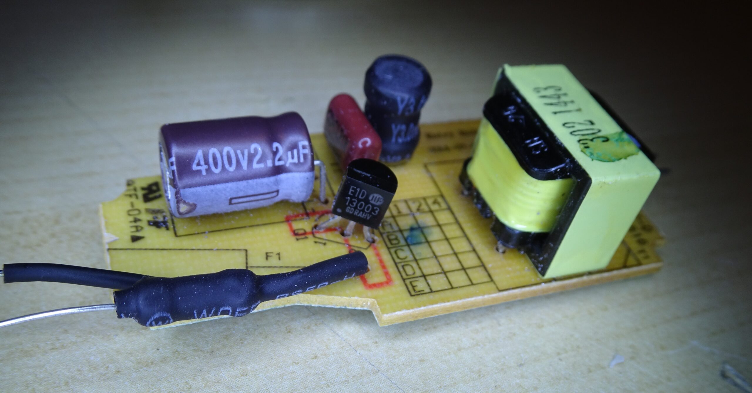
The PCB itself is a cheap, single sided type. On the top is a 2.2 μF electrolytic capacitor, a single transistor, a capacitor, an inductor and a transformer. Inside a piece of heat shrink is a 15 Ω resistor, probably a fusible resistor (one that also acts as a fuse).
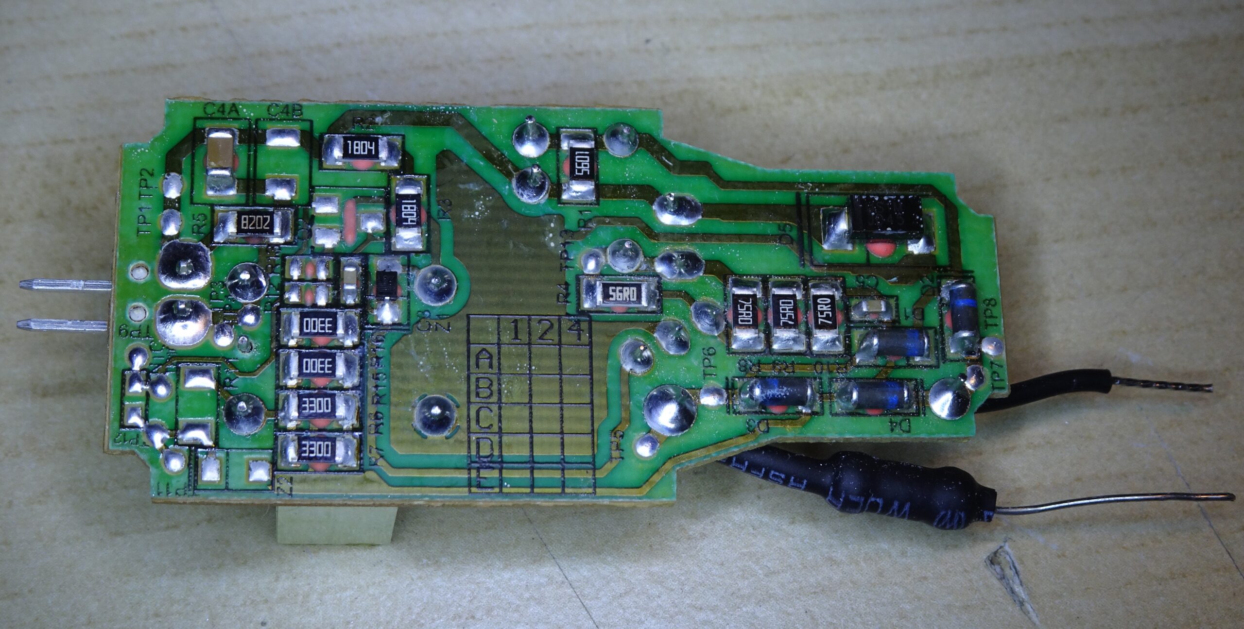
The bottom has more discrete components, all of them in SMD packages. This type of construction, where a single-sided PCB is used with SMD components on the bottom and through-hole components on the top, was quite common in the 1980s but fell out of use for anything but the cheapest products. The basic idea is to have a setup optimized for wave soldering: SMD components are attached to the PCB with glue (the red stuff you see under each component), through-hole components are placed on the other side, and then the whole assembly is placed above a tank of molten solder in which a horizontal wave is generated. The wave touches the entire bottom side of the board, soldering all components in one go.
As for the circuit, we can see four diodes (D1~D4) which rectify the mains voltage and buffer it on the large electrolytic cap. The transistor, together with the smaller capacitor and the primary side of the transformer, makes an oscillator that generates a high-frequency signal. The transformer’s secondary side will then generate a low voltage AC signal that appears to be directly applied to the LEDs. Some circuits are also present to regulate the output voltage and current, ensuring that variations in the mains voltage and temperature don’t affect the light output too much.
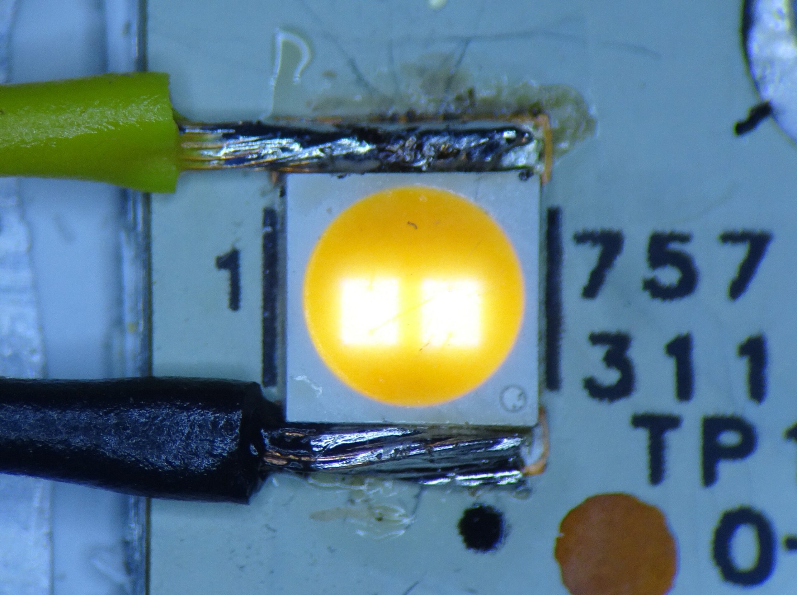
As it turns out, most of the LEDs still work. Up close, you can see that each LED contains two chips. In my broken light bulb, one of the five LEDs was completely broken, while another one had just one chip working. The light emitted is “warm white”, or slightly yellowish.
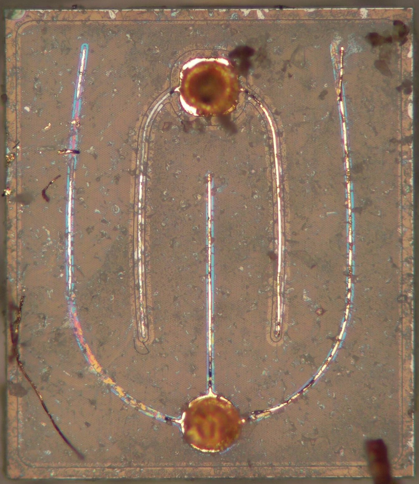
If we take the chips out of the package we find this interesting design. The anode (bottom) and cathode (top) are connected to the outside using gold bond wires. What’s interesting though, is that there are five wires spread out across the top of the chip that also look like they’re made of gold. These are clearly designed to make as much contact to the chip as possible without obscuring too much of the emitted light.
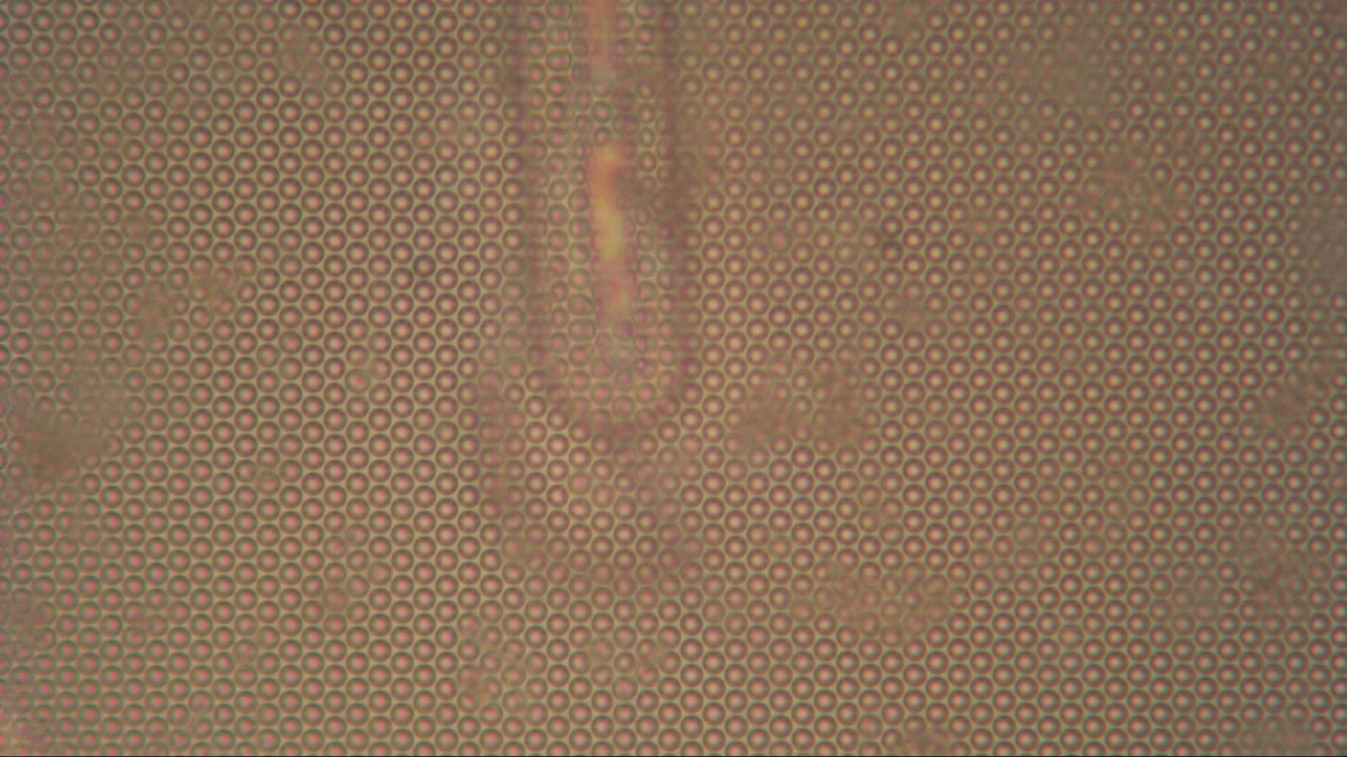
If we zoom in further, we find all these little spherical features spread across the entire chip. Perhaps these are little lenses to focus as much light as possible in the upward direction, similar to the lenses we saw on an image sensor a while back.
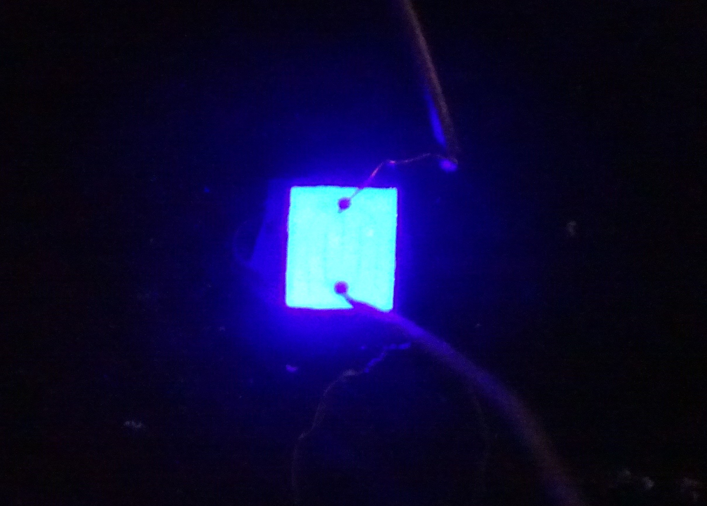
If we power up the bare die, it emits bright blue light. This makes sense, because LEDs by nature can only emit light of one single wavelength; white LEDs are made by encapsulating blue LEDs with a phosphor. Phosphors are materials that absorb light of one wavelength and emit light at another. By selecting the right type of phosphor, different colour spectra can be created from a single LED source. In our case, the phosphor is contained in the round yellow mass that sits on top of the LED chips.
To be honest, I was expecting to find some sort of custom chip inside this light bulb. But the only semiconductors on the PCB are diodes and a single transistor: apparently the relentless pressure to reduce cost has prevented the use of custom silicon. Instead, the bulb’s designers have managed to make the entire thing out of cheap discrete components, including this 3DD13003E1D transistor, a 400 V, 1.5 A NPN device made by Jilin Sino-microelectronics.
Two bond pads can be seen: in the bottom-left corner is the emitter contact, and at the top right is the base contact. The collector is formed by the chip’s substrate.
The emitter is formed by the little squares, contacted by the bottom-left bond pad. Surrounding the emitters is the base layer, contacted by the bond pad we see here. Together, they make the familiar N-P-N structure.
Hi, I am so sorry to bother you. If I was to send photos from inside an led light would you be able to tell me if all the components are normal?
Hi Victoria! Just looking at components doesn’t tell much, because they can be completely broken inside and still look fine. The only thing you can (sometimes) spot from the outside is fake components. The best way to tell if an LED bulb is ok is simply by turning it on. If it doesn’t, the only thing left is to replace it. Repairing a broken LED bulb is usually not possible or worth the effort.