The Apple TV is a media streaming device first introduced in 2007. It’s essentially a miniature Mac, running a special version of iOS optimised for playing music and video on a TV, and operated using a remote control. Although I personally have no need for such a device, I couldn’t resist when I found one for just €2.50 in a second-hand shop. It wasn’t that useful anyway since it was missing its remote control, not to mention the fact it was an old and unsupported third-generation model, sold between 2012 and 2015. But it presented a very good opportunity to tear down some modern Apple hardware and get an up-and-close look at their custom silicon.
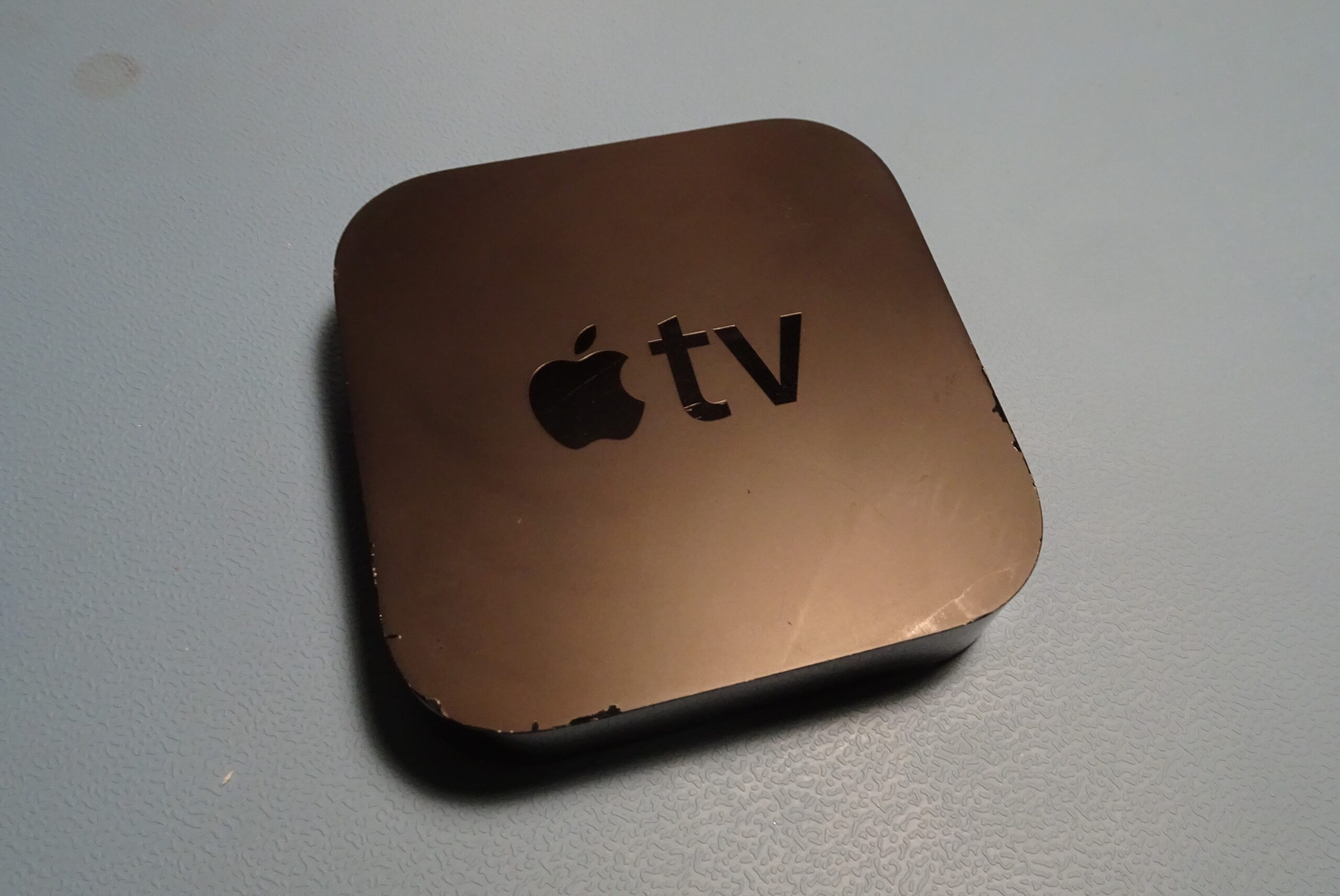
The design of this box is sleek and minimalist, as we might expect from Apple. The top and sides are simple black plastic, with all connectors located on the back.
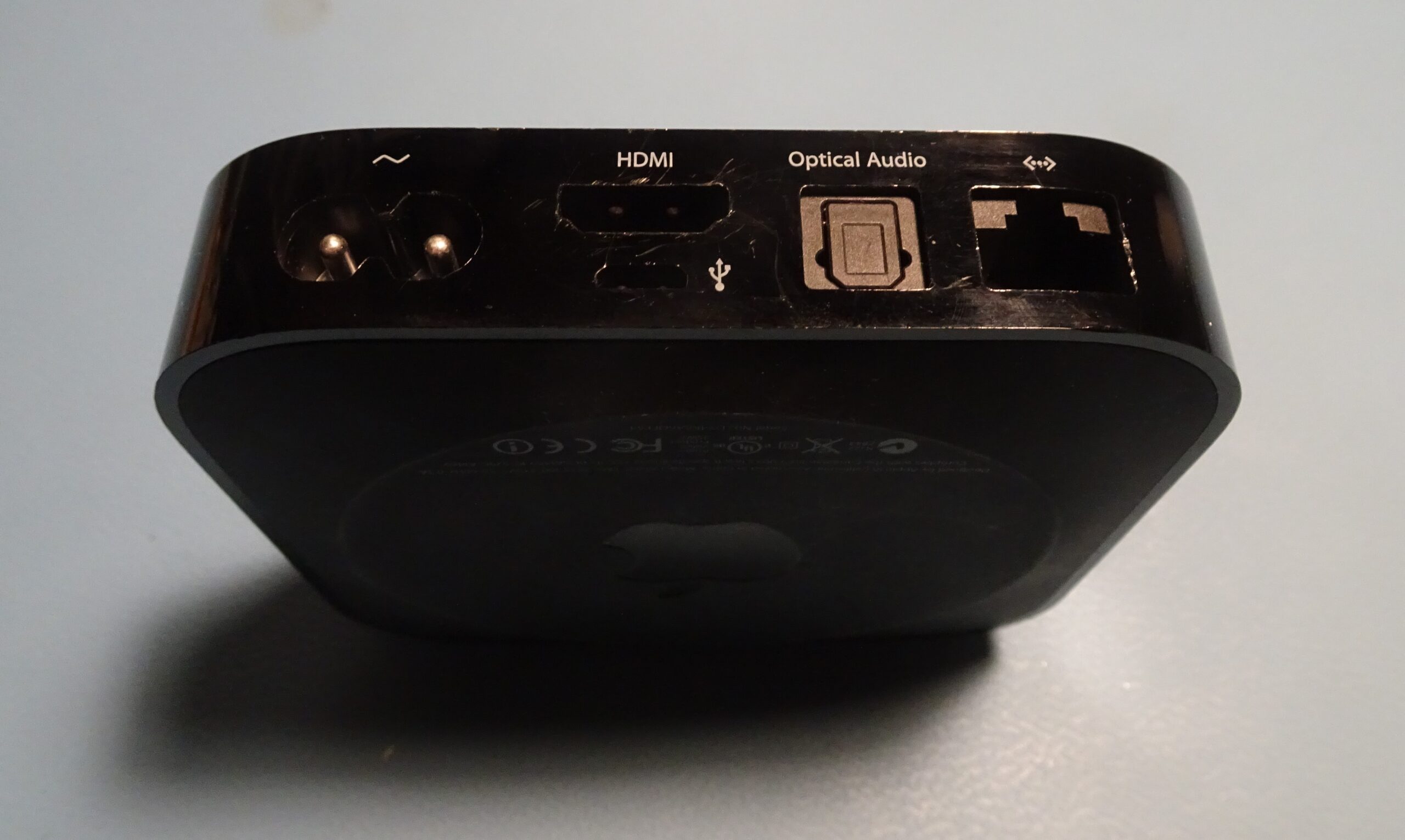
From left to right we find a mains power connector, HDMI, USB, Toslink optical audio and an 8P8C Ethernet connector. Inside there’s also a WiFi and Bluetooth interface, and an IR receiver looking out the front.
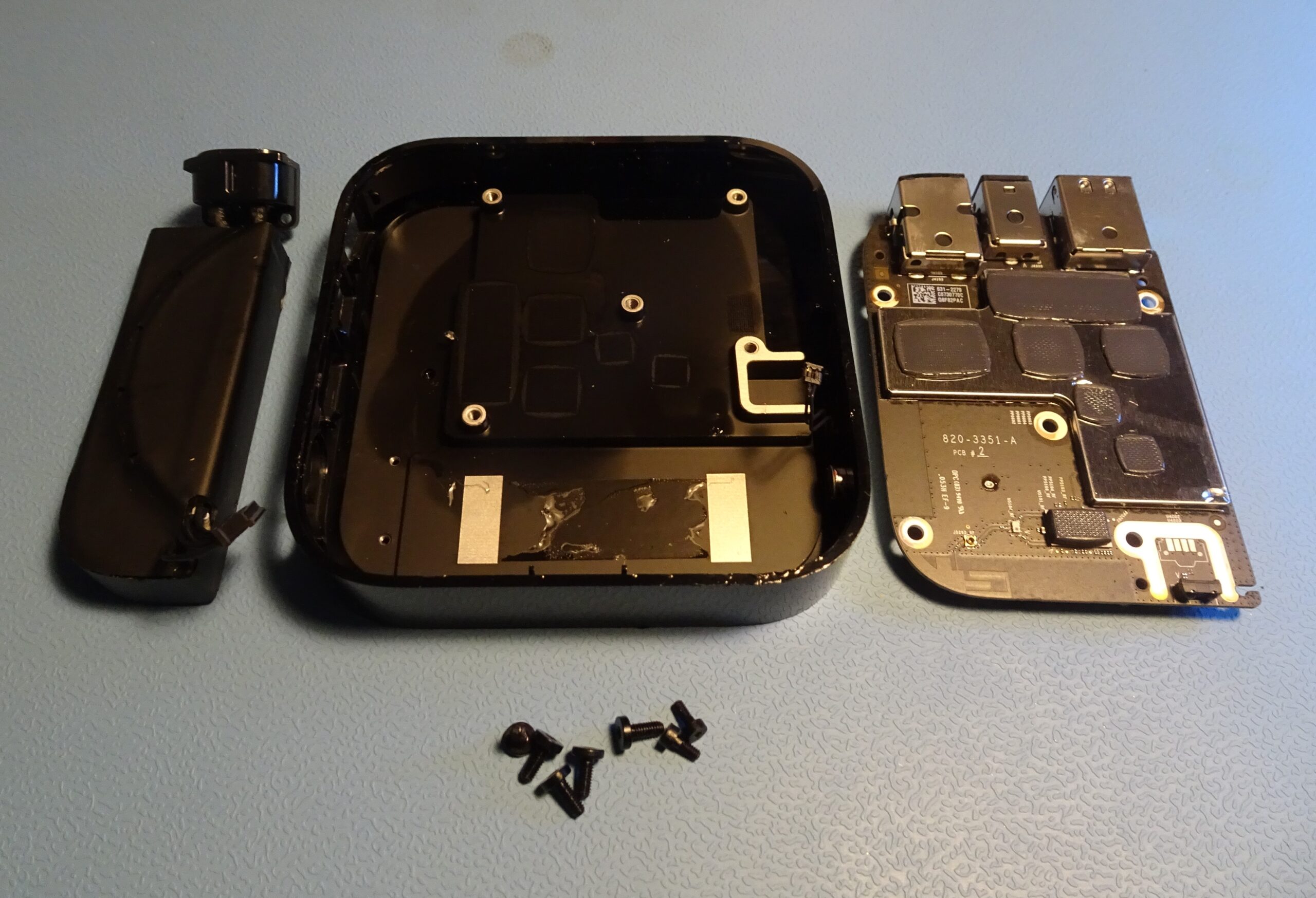
The whole system is held together with a handful of Torx screws. There’s a very compact power supply and a single black circuit board holding the CPU, memory and interface chips. The top of the case is filled with a big chunk of machined aluminium acting as a heat sink.
This is what the boards look like when we remove the thermal pads, RF shields and other packaging. The main black PCB has three big chips holding (from left to right) flash, CPU and RAM, plus two smaller ones below for WiFi and Bluetooth. We can also see the infrared receiver at the lower edge. The power supply is made on a regular green board, with lots of white anti-vibration goo.
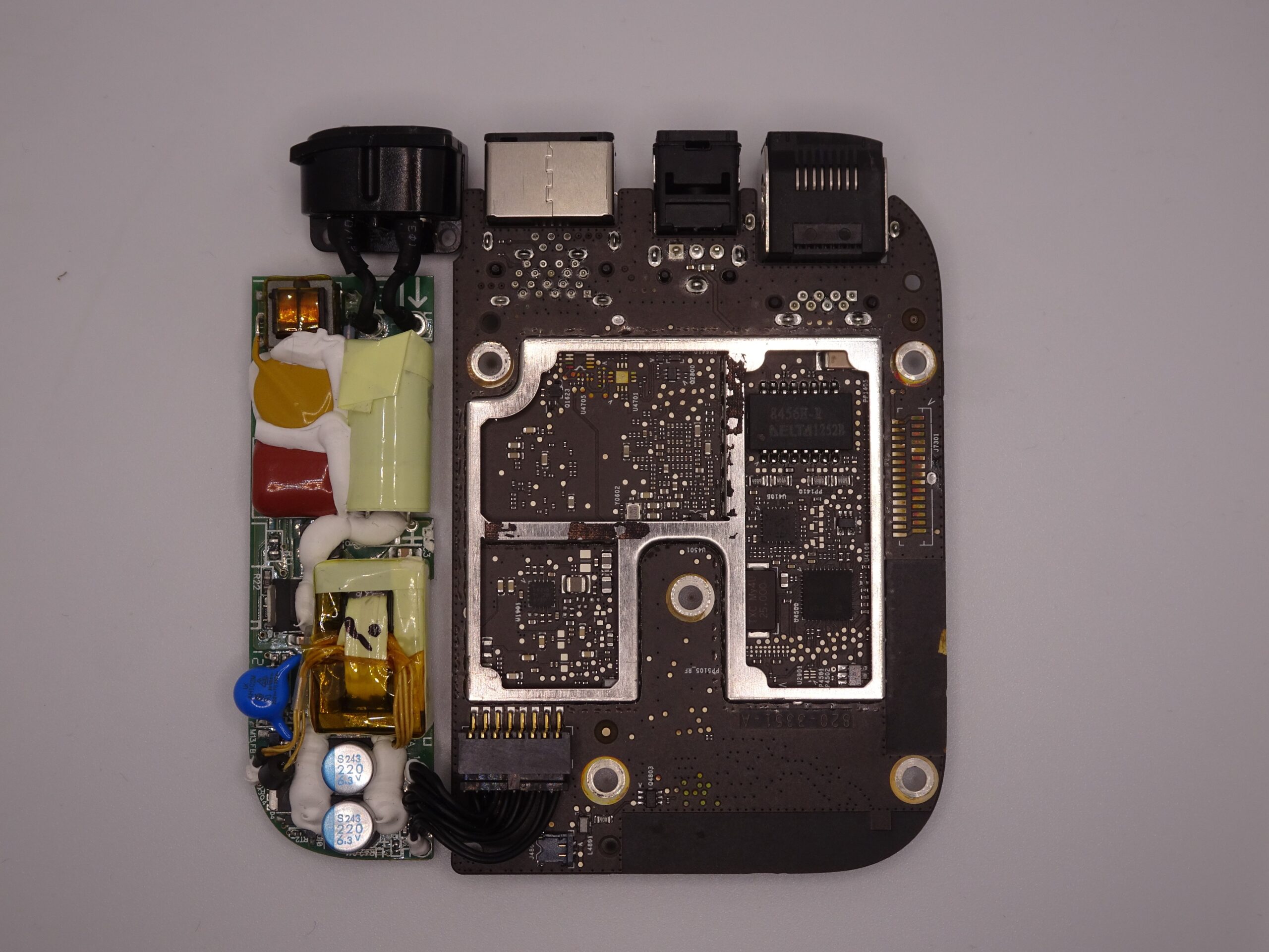
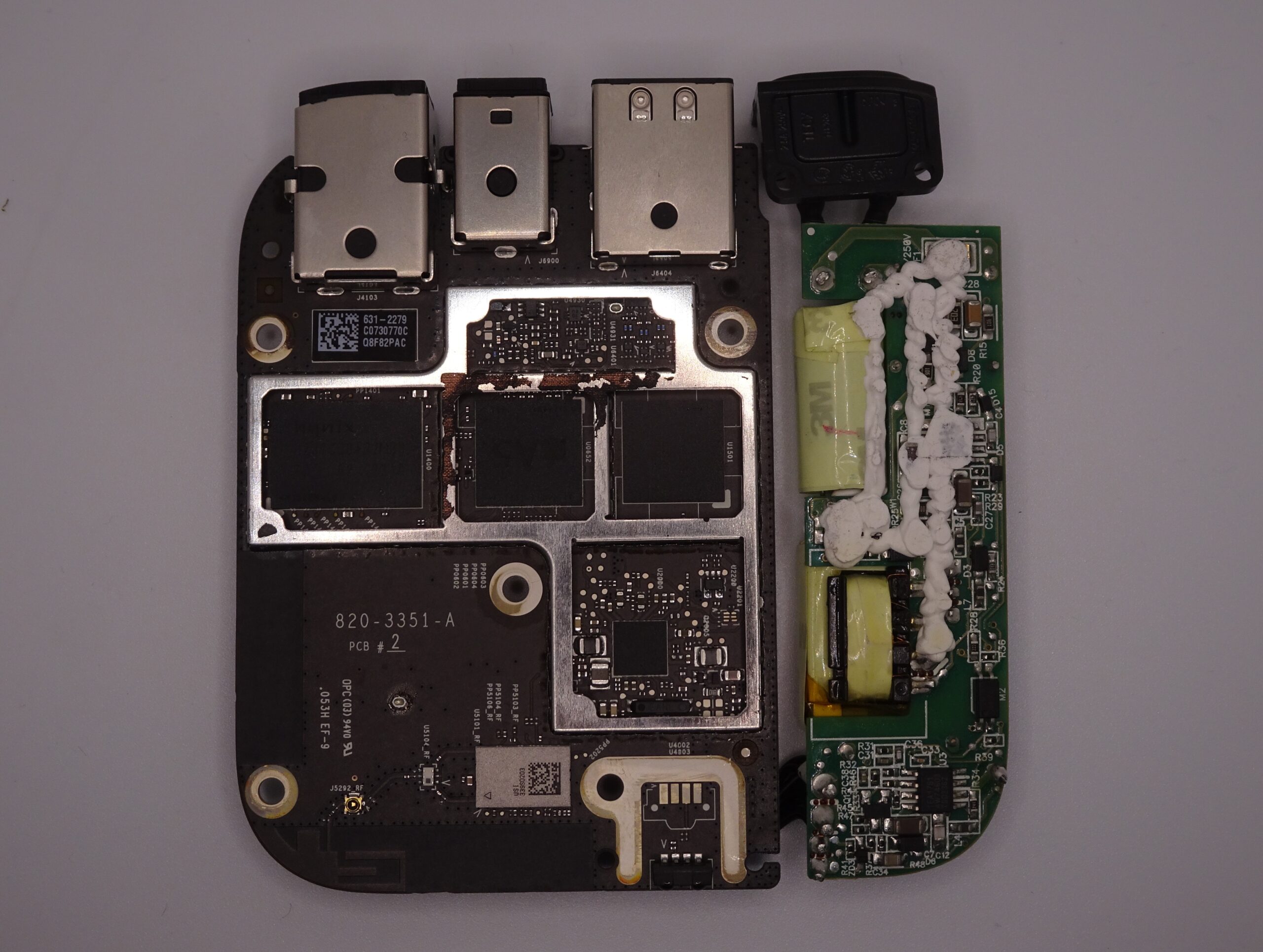
The other side has an Ethernet section as well as a power management chip. We can also clearly see how the mains power connector (on the top left) and the Ethernet connector (top right) are designed to follow the curvature of the case. So instead of slightly adapting the position of the connectors, or just modifying the shape of the case a little, Apple decided to get customised connectors to fit their design. No engineer would have made that choice, or got away with it, at any regular company, but Apple plays by different rules. Because, you know, they’re Apple.
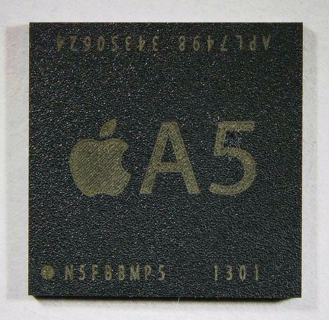
Today we’ll look at the chips on the main PCB’s top side, starting with the Apple A5 CPU. This is a single-core 32-bit ARM Cortex-A9 processor with an integrated PowerVR graphics processor. The “APL7498” marking at the top indicates that this is the second-generation version of the A5, manufactured in a 32 nm process.
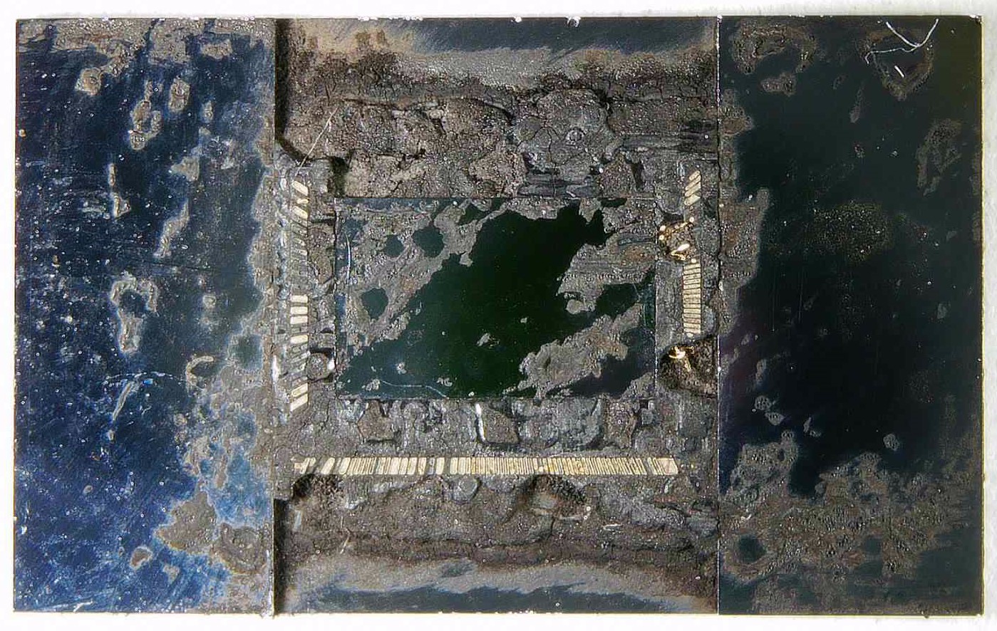
The chip is housed inside a 23×23 ball BGA package. When we remove the package, we find something very similar: a flip-chip die with several hundred solder balls. Basically, the flip-chip die is mounted onto a small PCB called an interposer, which spreads out the signals to a larger grid of solder balls. This makes it possible to re-route the signals so they can be easily routed on the main PCB without having to make complicated wiring on the (expensive) chip layers. It also means that only the interposer has to be made to a very fine resolution, and not the main PCB.
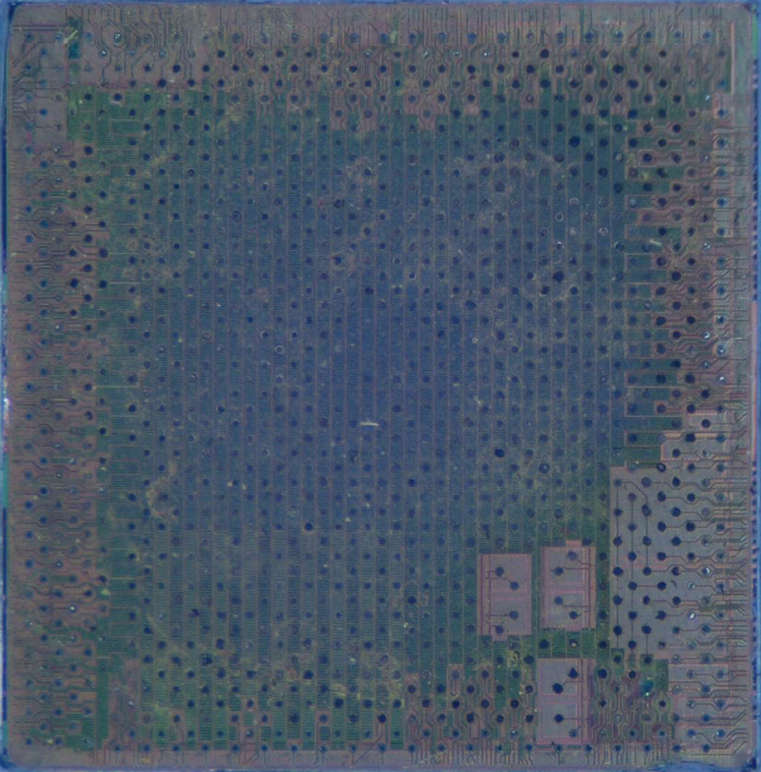
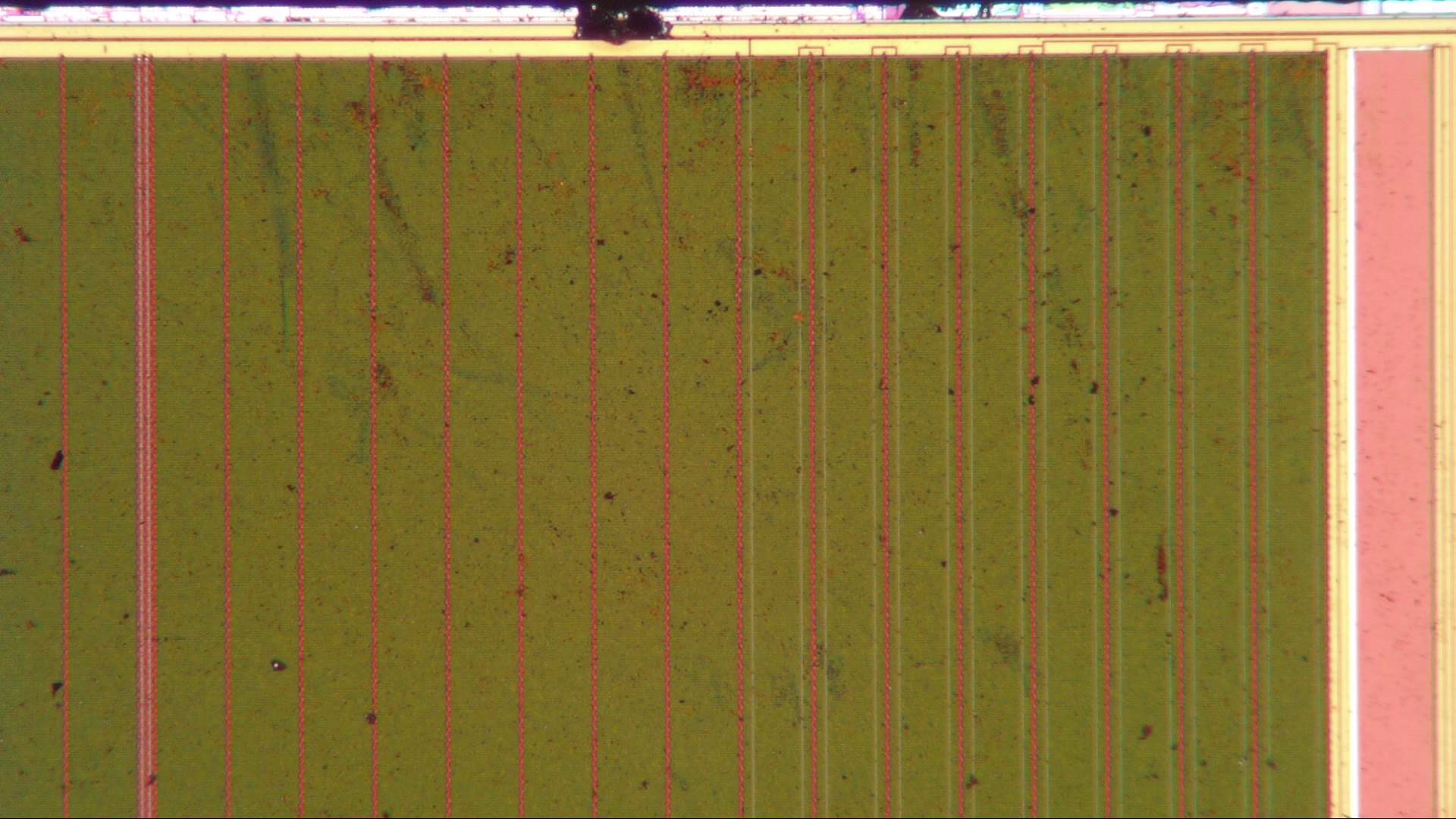
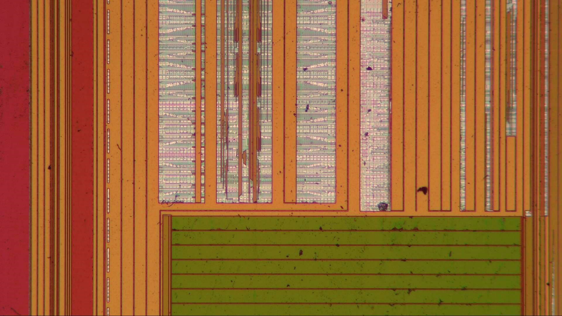
The pads holding the solder balls (called bump pads) are clearly visible when we zoom in a bit. The ones we see here mostly carry signals. A few on the left clearly carry differential signals, given how they try to keep the length of two traces more or less equal.
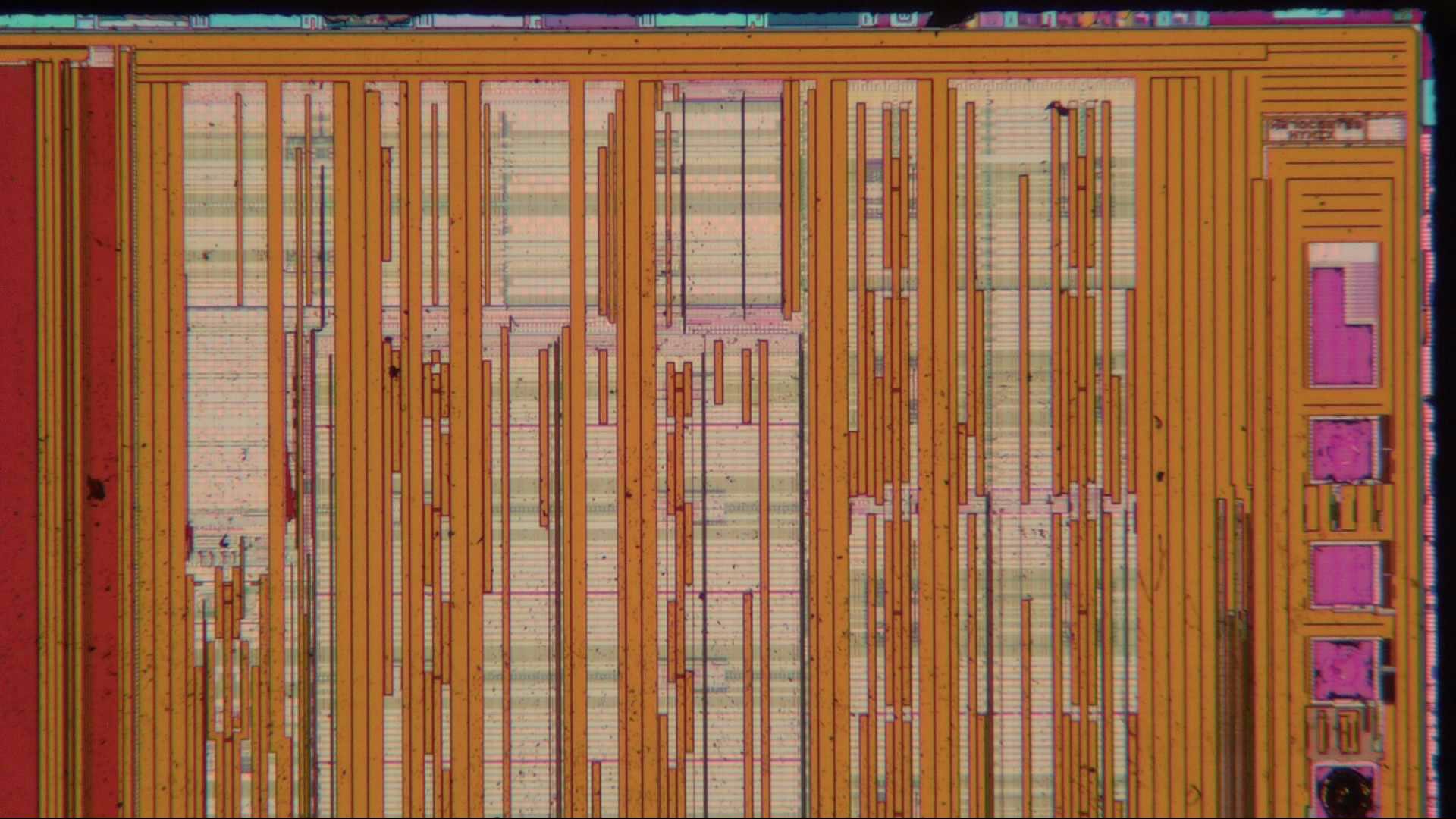
Most of the pads are carrying power, however. Thick vertical bars carry VDD and VSS along the top metal layer, with lower layers distributing power left and right. The power grid is only broken in a few places, like shown here, where other signals had to be routed down into the main circuitry.
Sadly, we can’t really see much more than bump pads and power routing since those take up the majority of the chip’s area. What’s left is mostly covered with dummies: little squares of metal that fill up any empty areas to ensure an even thickness of the metal layer all across the chip during etching and polishing.
There aren’t any logos or markings anywhere on the top layer. In fact, I find it a bit annoying that we can’t really see anything on these types of chips, so I’ve started researching ways to remove the top layers and hopefully be able to peer down a bit further than we can now.
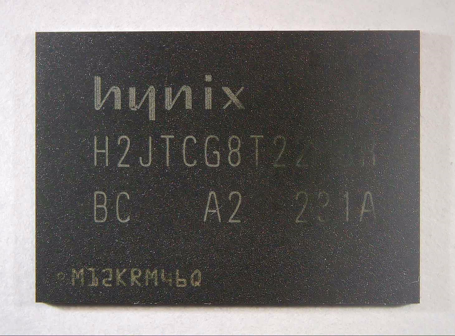
Next up is the flash chip, a Hynix H2JTCG8T22MBR. It’s a 64 Gbit NAND flash chip, manufactured in a 2y-nm class process. This means it’s a twenty-something nanometre process, without specifying any exact feature size.
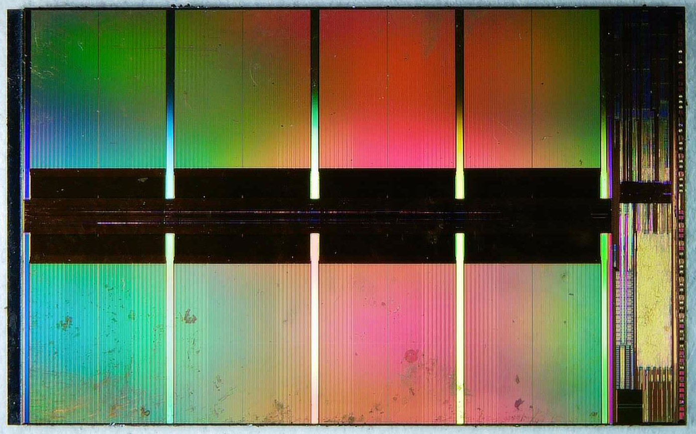
The chip inside, which is almost the same size as the package, looks like this. Large arrays of flash memory cells give a pretty rainbow effect under the microscope.
However, there’s more than just the flash chip. The whole thing is actually a stack of four pieces of silicon: the big flash chip shown above, a smaller chip mounted on its back, and two rectangular chips mounted on either side of the small chip. I’m not sure if those two contain actual circuitry or if they’re just there for mechanical support; I’ll have to take this stack apart a bit further to figure out what’s what.
For now though, we can already see some beautiful circuitry on the main die. There aren’t any dummies or unnecessary metal on the top layer, so we can actually see some stuff over here in the readout section of the chip.
The memory section is, as we might expect, a sea of identical cells covering most of the chip.
At the edge of the memory section are these tree-like structures typical of address decoders.
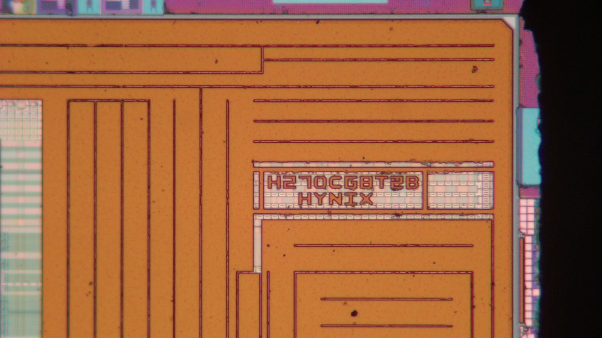
A little marker tells us that we’re looking at an H270CG8T2B made by Hynix. This is the part number of just this chip; the part number printed on the package refers to the entire stack of chips.
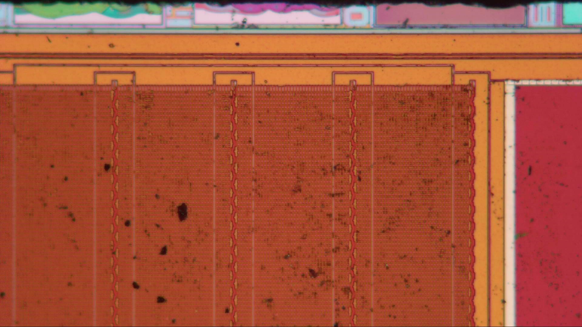
If we zoom in on the memory array we find these interesting stacks with a zig-zag pattern in the vertical direction.
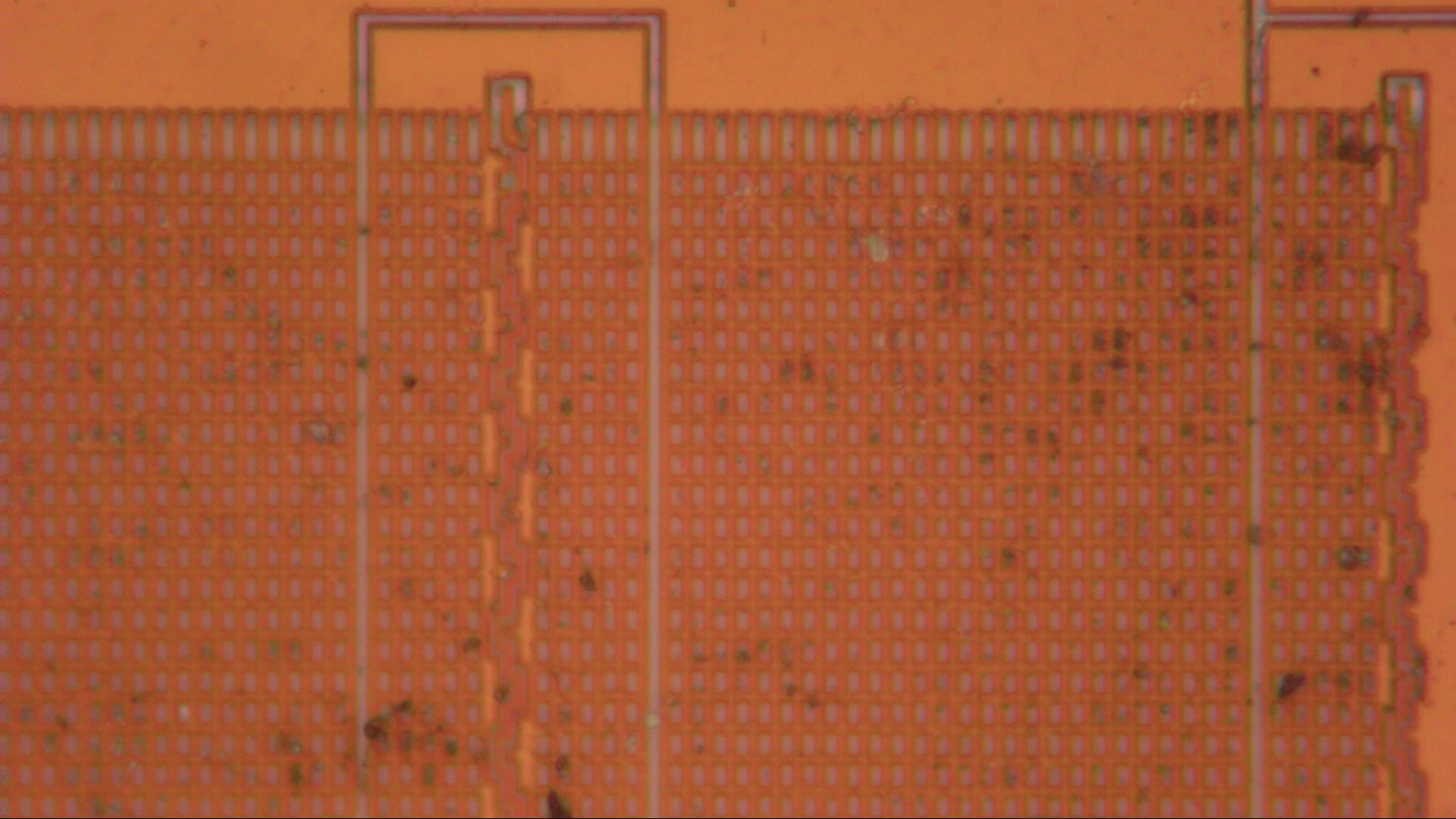
At maximum magnification we can just about see a grid of cells. We definitely can’t see the actual memory cells: 20-odd nanometres are way too small to see with an optical microscope.
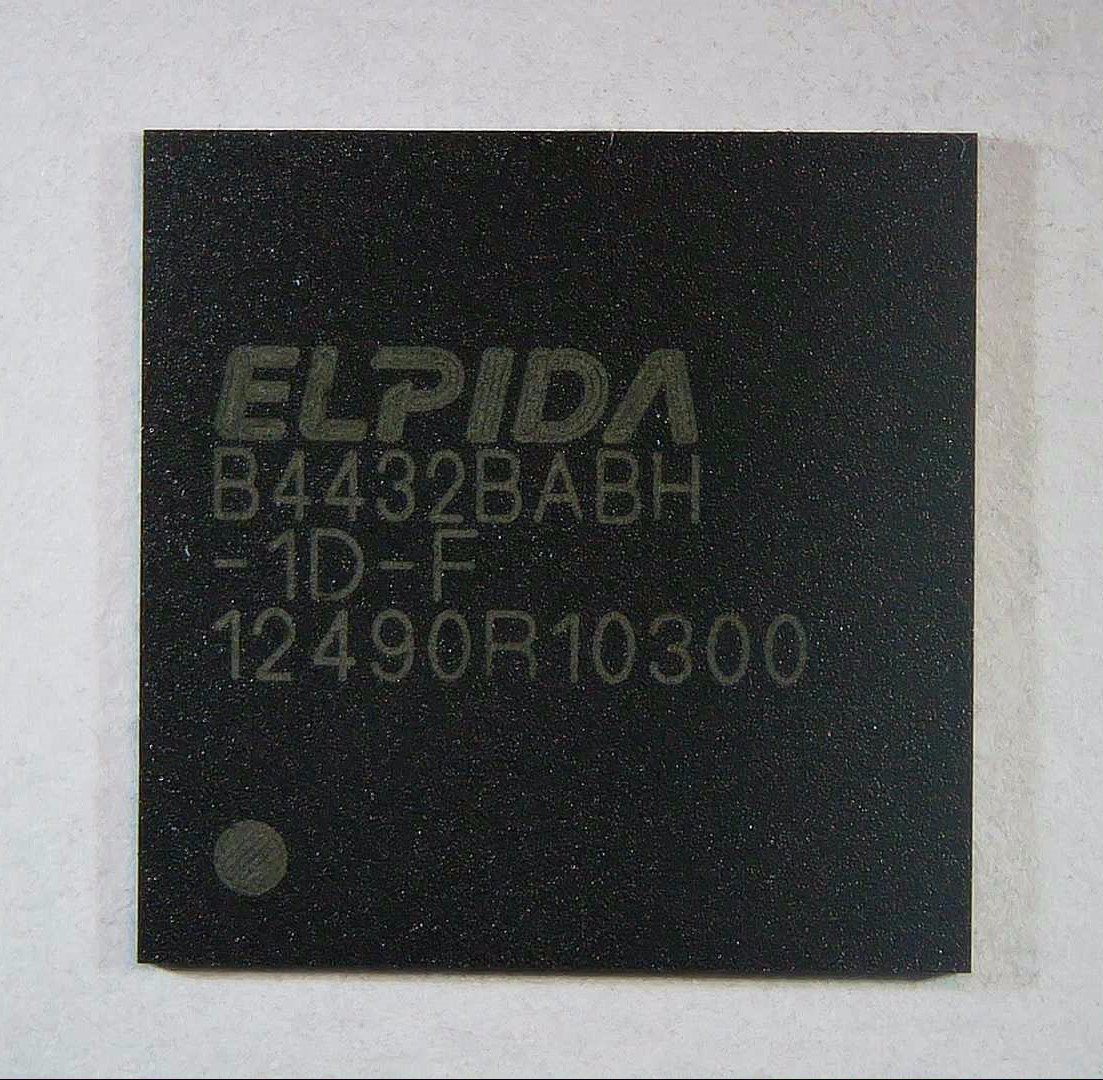
The third main chip is the B4432BABH-1D-F made by Elpida, containing 4 Gbits of LPDDR2 memory running at 533 MHz. Elpida was formed from Hitachi, NEC and Mitsubishi’s memory units around the turn of the century, but failed to become profitable and was eventually acquired by Micron Technology in 2013. This chip must belong to the final batch of products bearing the Elpida logo.
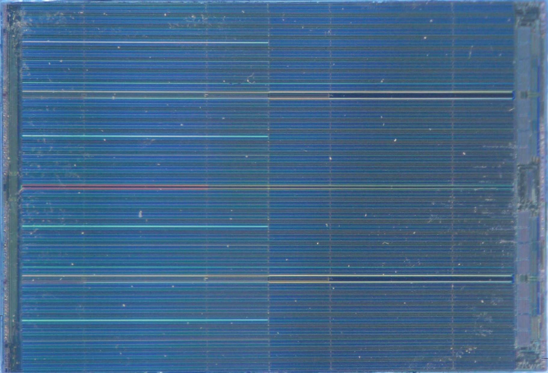
The chip looks exactly as you’d expect from a memory chip: a large grid of identical cells. It’s also way too big for my metallurgical microscope, which is why I’ve taken this picture through my stereo microscope (as I did with the flash chip and the CPU).
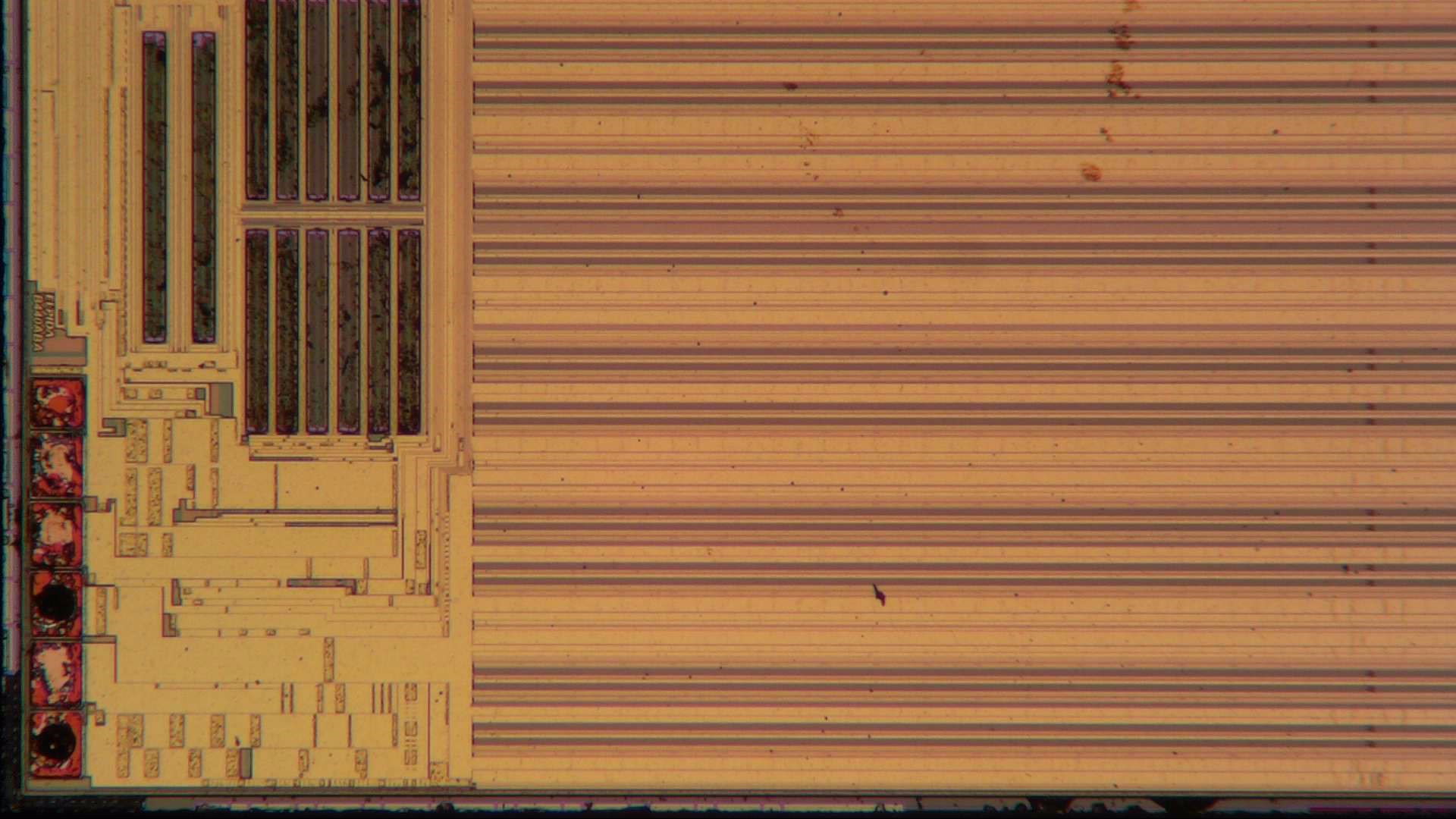
Up close, we find some readout circuitry on the left, a handful of bond pads, and the memory array itself.
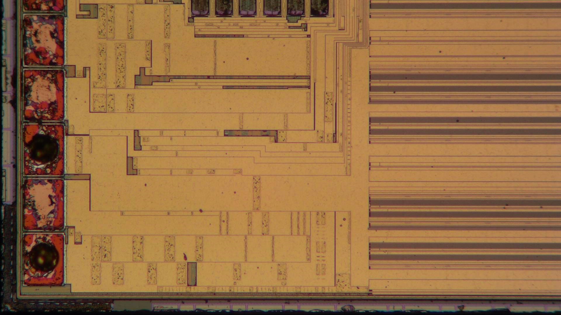
Again, the circuits below are largely obscured by metal. No dummies, though: the metal wiring is simply wide enough to neatly fill up the whole area.
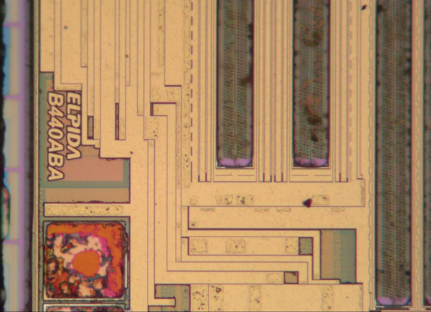
Elpida’s engineers have helpfully indicated that we’re looking at a B440ABA chip, though they didn’t include a copyright date. Again, being able to remove the top layers would be helpful to see more of the internal circuits.
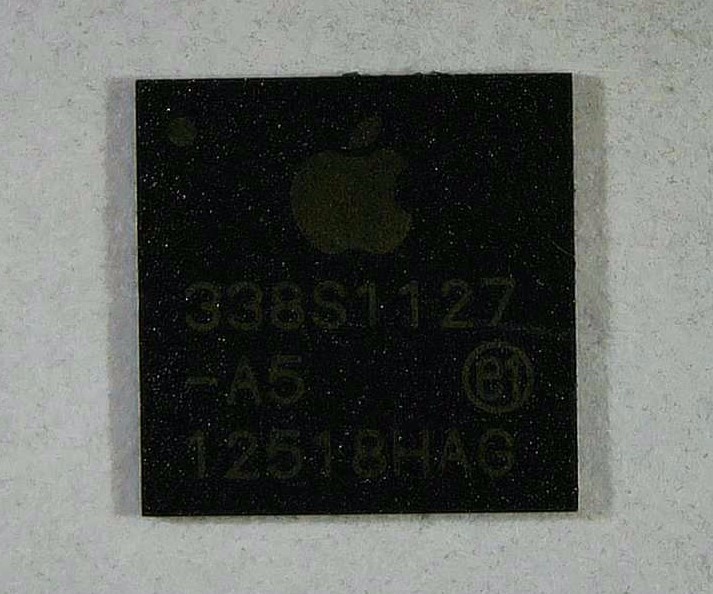
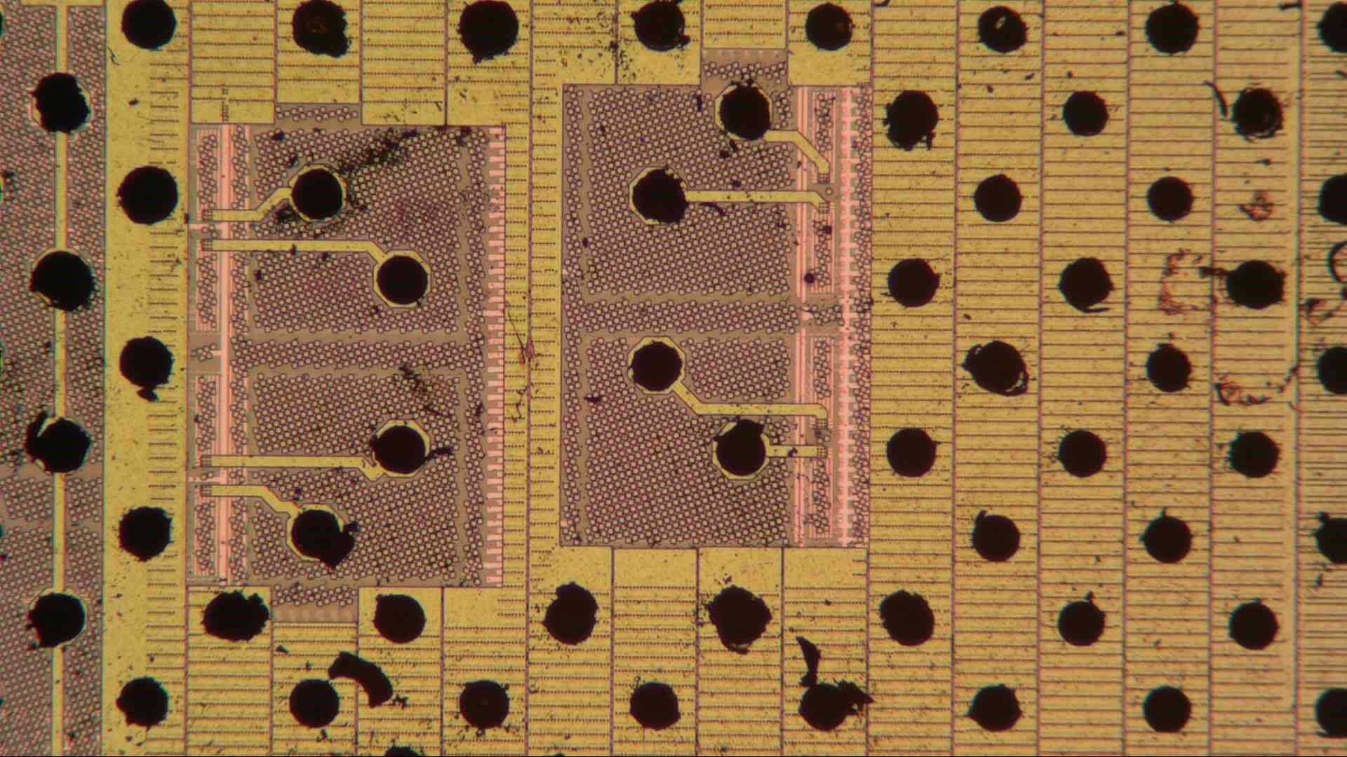
Next, we’ve got another piece of custom silicon made for Apple, labelled 338S1127-A5. This is a power management chip designed for the A5 CPU.
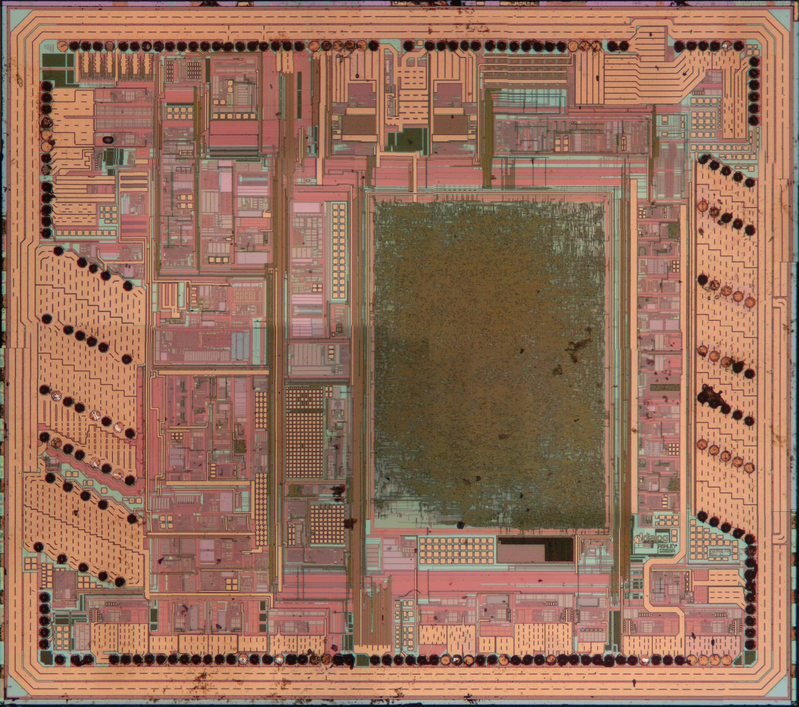
Inside, we find this pretty mixed-signal power design. There’s a block of digital logic in the middle, power transistors on the left and right edges, and lots of analog circuitry in between.
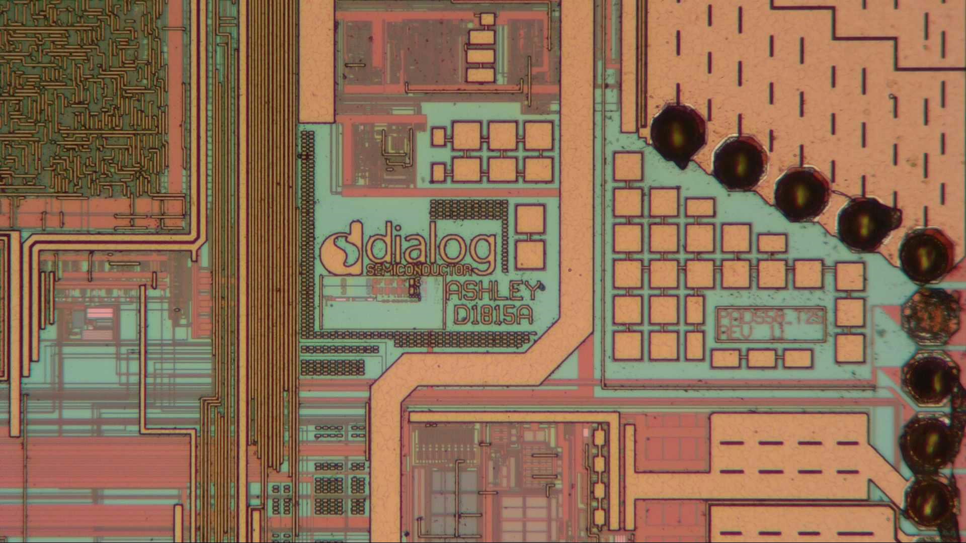
The internal code names of this chip seem to be “Ashley” and “D1815A”. It was made by Dialog Semiconductor, which was Apple’s main supplier of power management chips at the time. Apple eventually purchased the power management division and integrated it into their own organisation. What was left of Dialog was later acquired by Renesas.
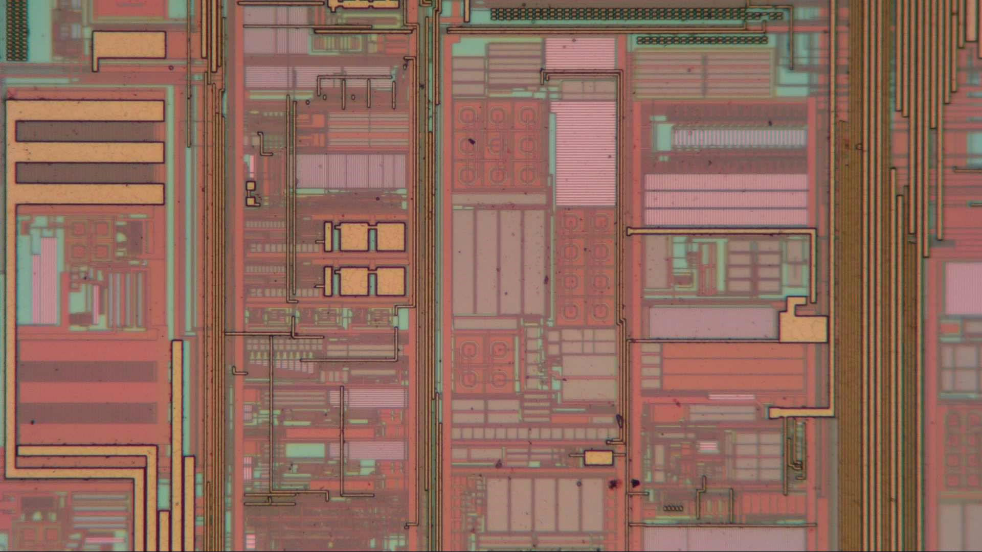
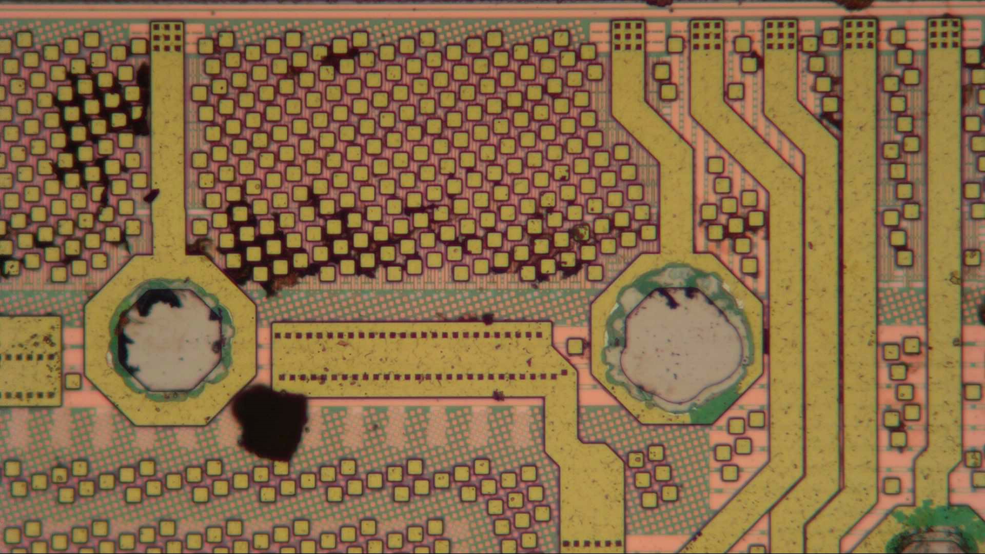
A large part of the chip is filled with analog circuit blocks like these. We find big transistors and resistors, probably a bunch of capacitors as well, and several groups of bipolar transistors (red squares with circles inside).
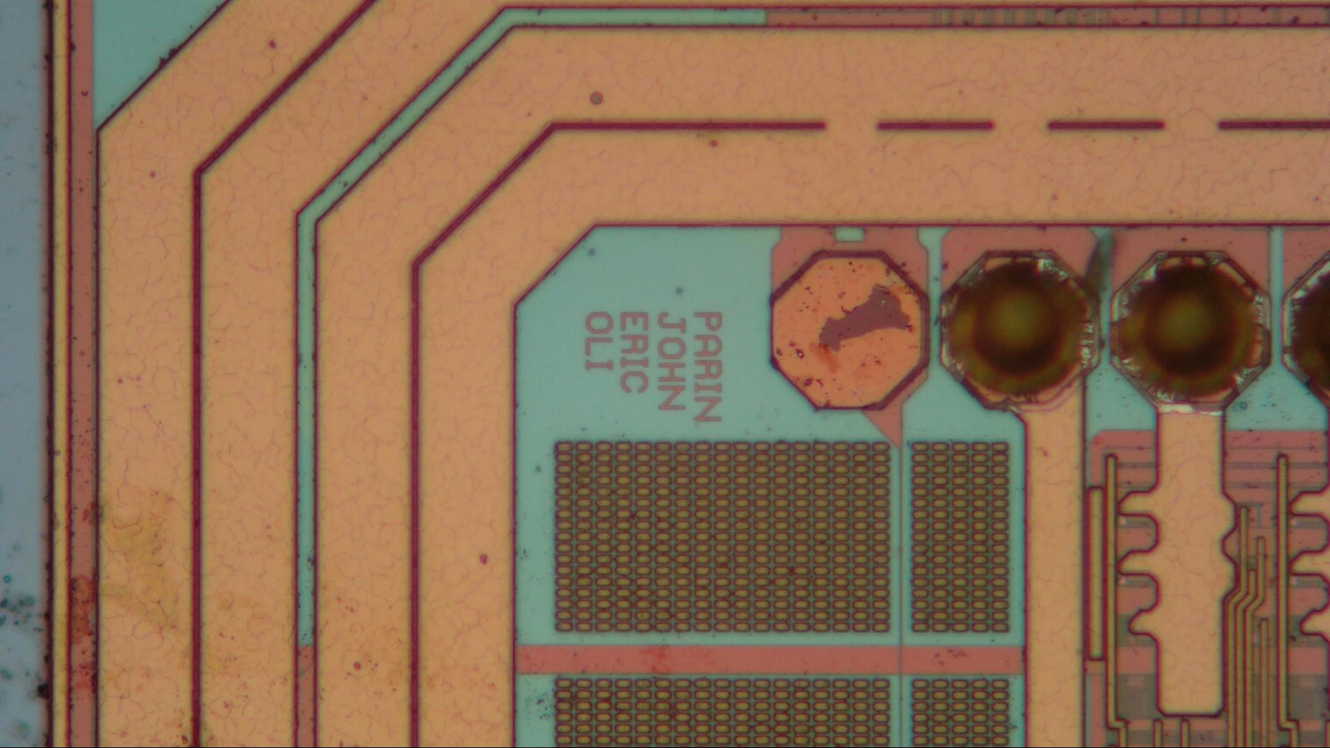
Up in this corner we find the names of some of the engineers who worked on this design: Parin, John, Eric and Oli. We also clearly see two wide wires running around the outside of the chip, which are most likely a VDD and VSS wire. They have slots down the middle to prevent mechanical stress from building up inside them. Typically, design rules state a maximum allowed width for metal wires in each layer that takes this into account.
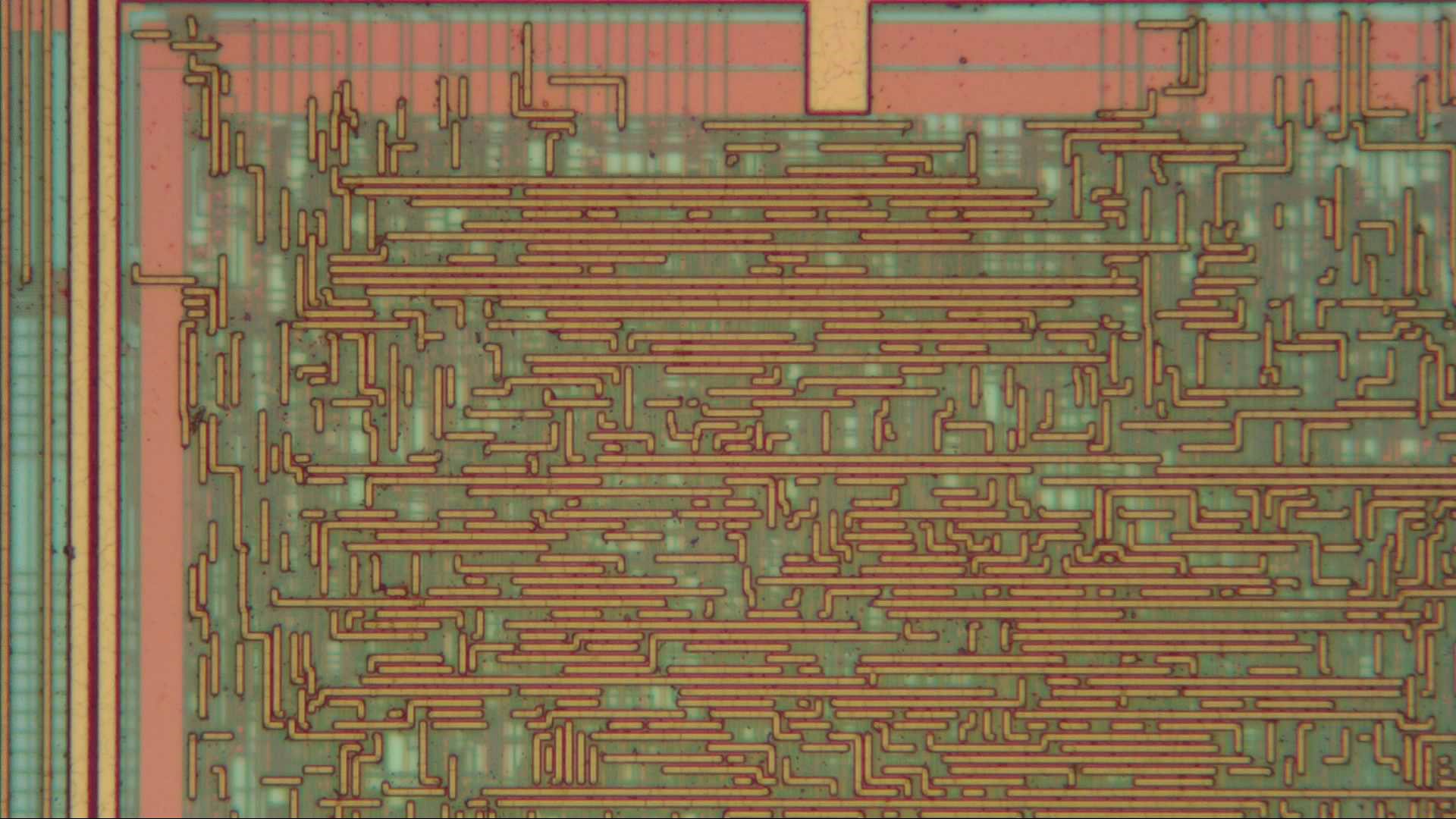
The digital block is not very dense. It’s clear that this chip was made in a much less advanced process than the CPU and memory chips. Power management chips are commonly made in processes based on older digital nodes, with additional layers to create power transistors and higher-quality analog components.
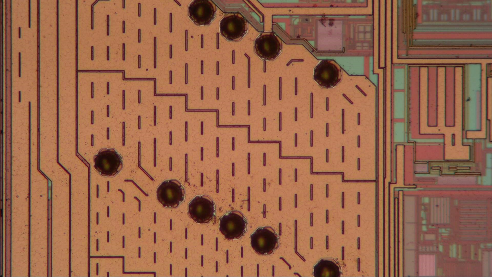
Those power transistors are below these large pieces of metal. There are several bond pads to spread the current across multiple bond wires and reduce the resistance. The metal is again slotted all over the place to reduce stress.
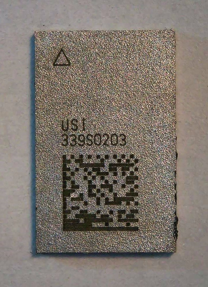
Finally, there’s an RF interface chip labelled USI 339S0203. Apple’s custom chips apparently have part numbers based on three digits, the letter “S”, and another four digits. The Data Matrix below the part number contains the string 21036005790213012200179139, which is probably a serial number.
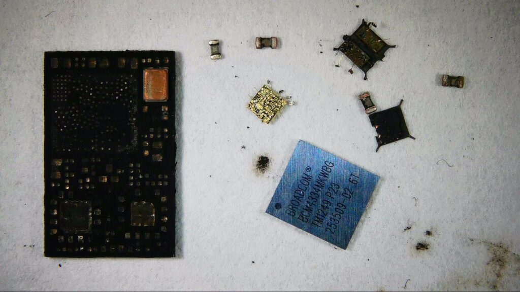
The USI device isn’t a single chip; it’s actually a small PCB containing several chips and passive components, all encapsulated in grey plastic. The picture above shows what’s left after taking it apart: three chips, a crystal oscillator and a bunch of passives. One of the chips is helpfully labelled “Broadcom BCM4334”, which tells us it’s a WiFi/Bluetooth/FM radio device. There’s also a smaller square chip, and a third one (top right) that contains two separate dies.
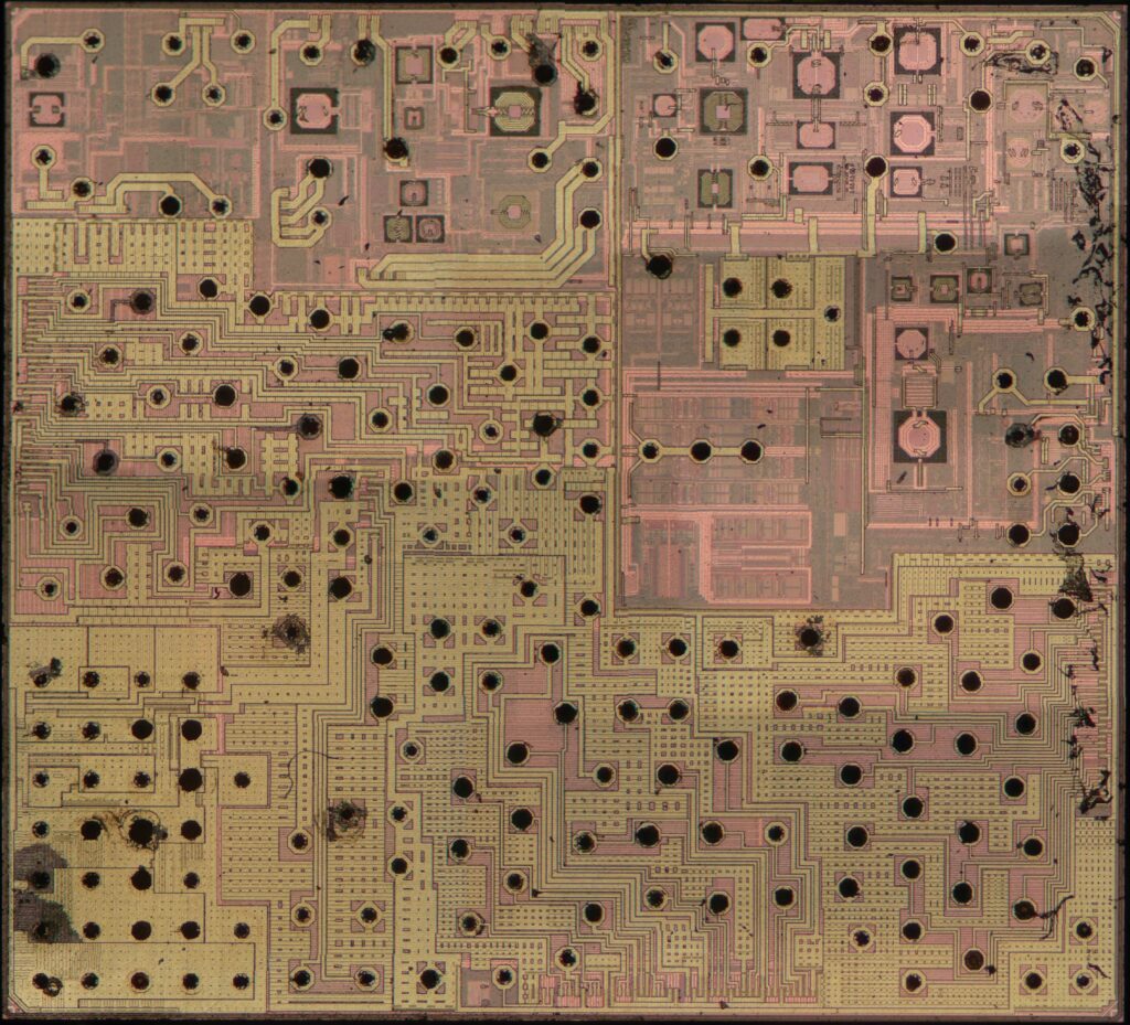
Starting with the big Broadcom chip, we again find a flip-chip device with lots of solder balls. The circuitry is divided into clear blocks: on the top left is the FM radio, which is probably unused in the Apple TV. To its right is the Bluetooth block, which is used for interfacing with peripherals like the remote control. The block at the top right (taking up about a quarter of the chip) is the WiFi radio. Bottom left is the local power management module, with the rest being used by digital blocks for the radio interfaces and an ARM Cortex-M3 core.
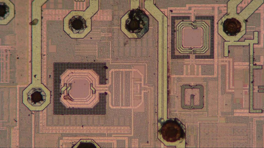
If we zoom in a bit, it immediately becomes obvious that this is an RF chip: there are on-chip inductors everywhere. They are often used to create oscillators and filters, and to tune the bandwidth of amplifiers. On-chip coils only work well at signal frequencies of about 1 GHz and above, which is why you don’t usually see them in things like FM radios and other things that work at 100 MHz and below. The ones seen here belong to the Bluetooth radio.
Here we’re looking at the boundary between the Bluetooth block (left) and the WiFi system (right). Note how the top metal layer (which appears yellow in these pictures) doesn’t require any dummy structures: the only shapes we see are are wires and coils. The layer below however (which appears pink), is filled with dummies, though not at critical locations such as inside the coils. This is usually allowed, though at the cost of slightly lower accuracy of nearby metal features.
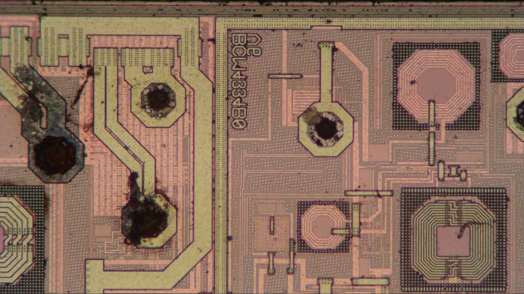
Also interesting is that we find mirrored text reading “BCM4334B0, V6” in the corner of the WiFi block. It’s possible that this block was originally designed the other way around, but that it was discovered later on in the design process that flipping it made it fit better in the overall floorplan. Since electrons don’t care which direction they’re flowing in, this doesn’t have any effect on circuit performance.
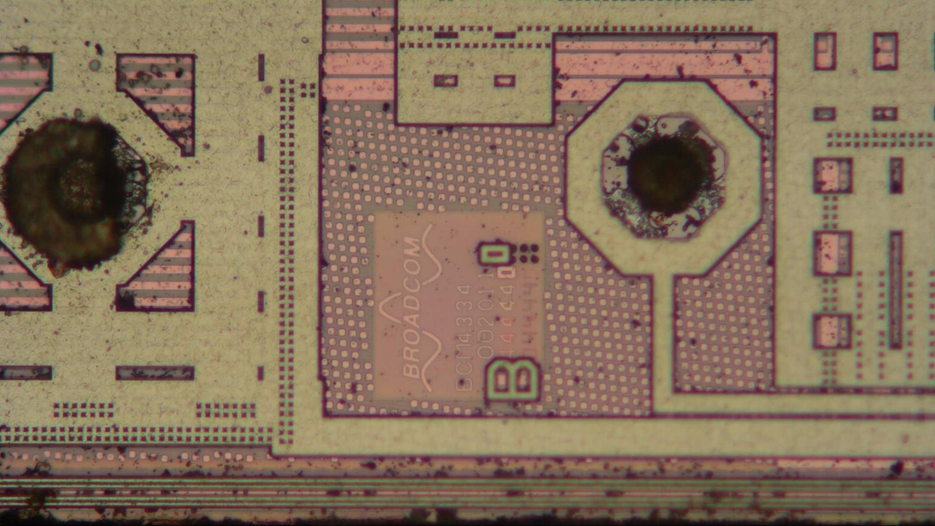
At the bottom edge of the chip we find the Broadcom logo, non-mirrored this time, along with the chip’s name and some revision letters.
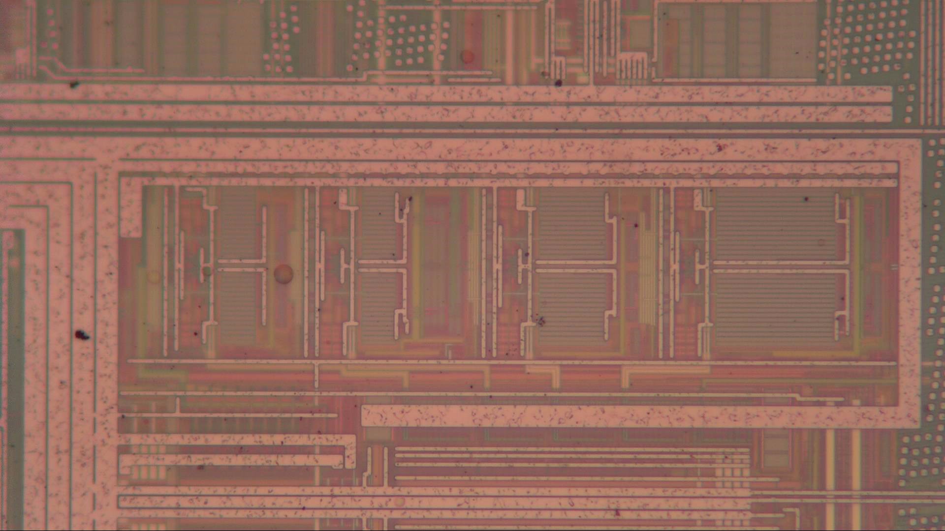
The circuits between the RF coils consist of general analog circuitry such as amplifiers, switches, A/D and D/A converters. What we see here looks like a differential ADC or DAC, with similar circuits that become larger as we move from left to right.
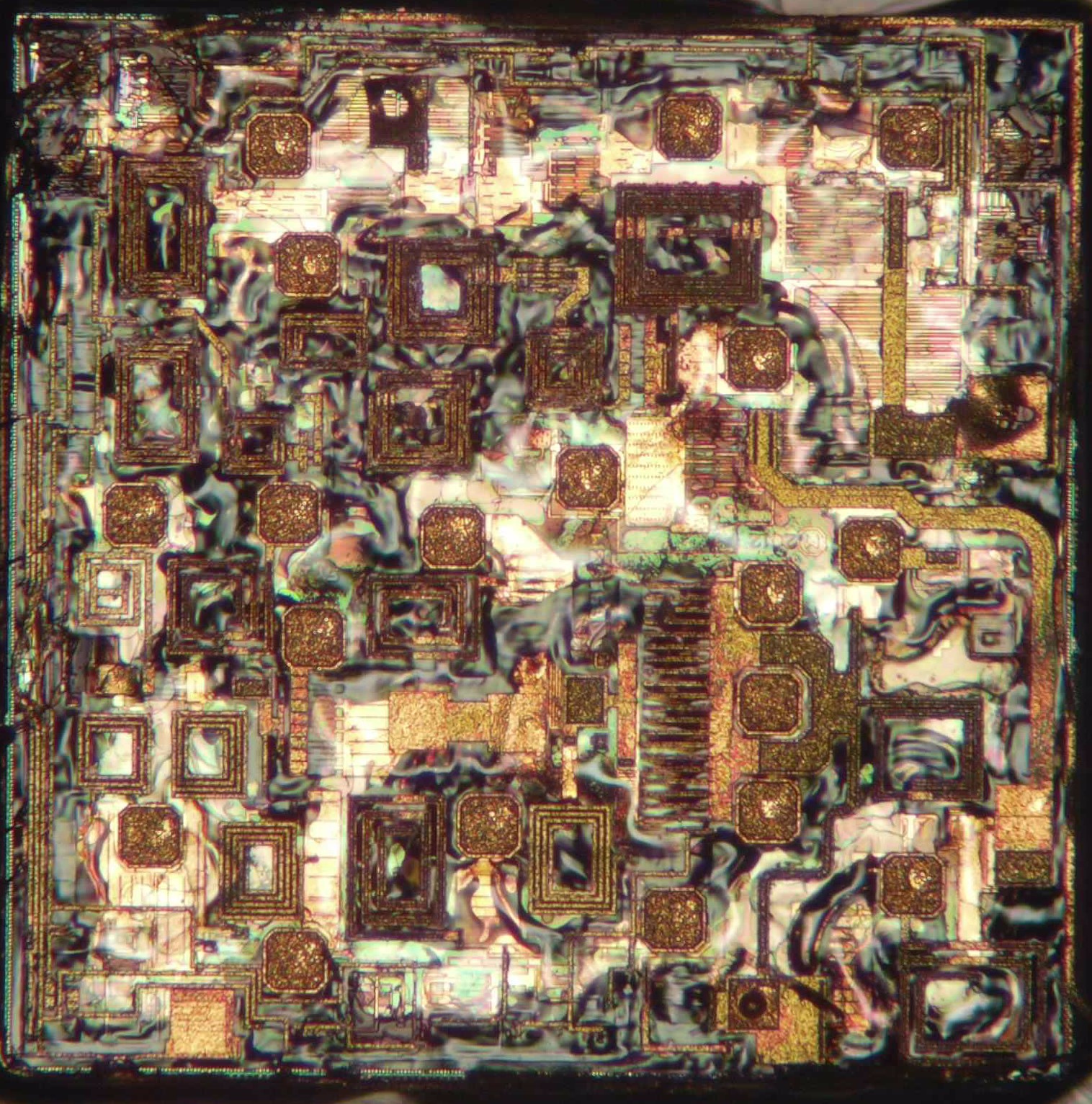
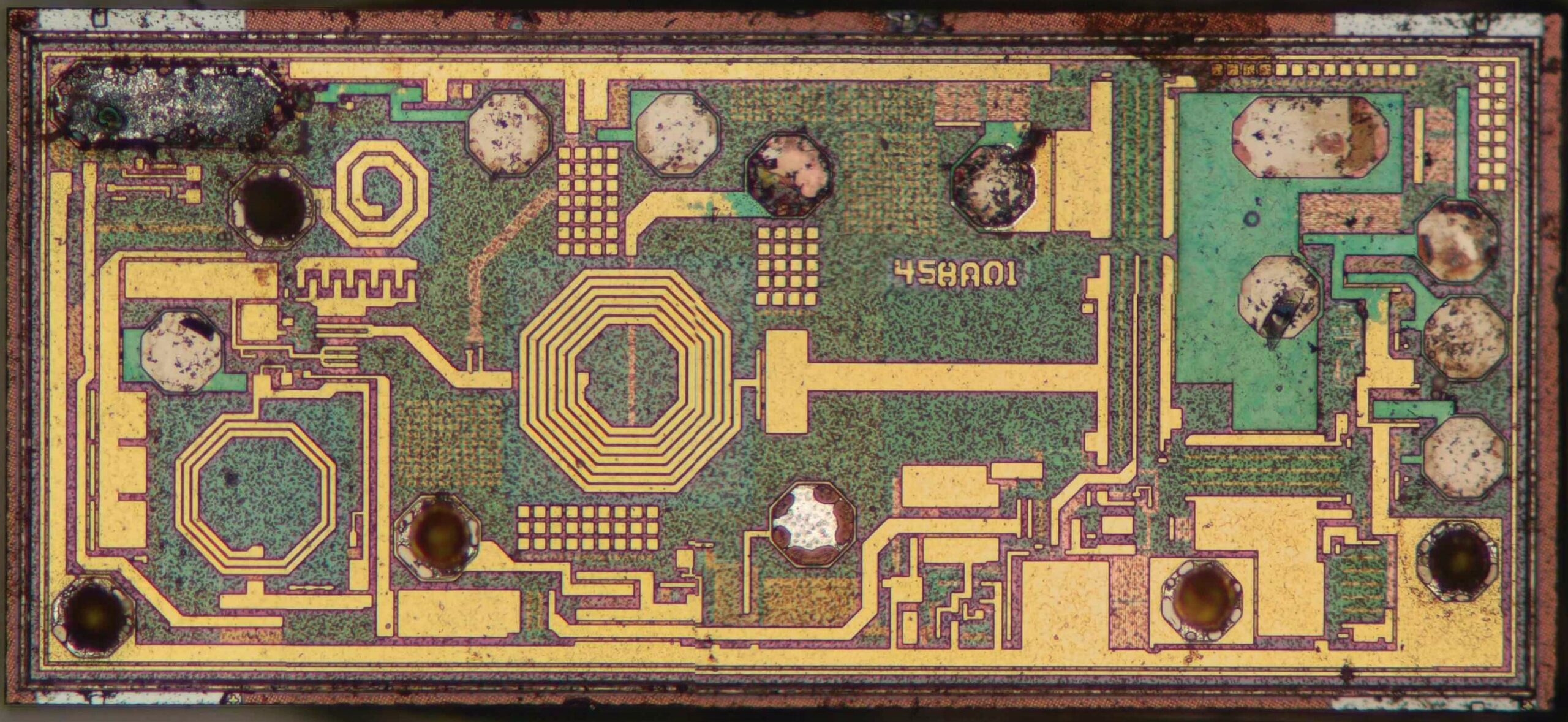
The second chip inside the WiFi package is this weird thing: it’s a small chip, clearly with lots of RF functionality inside, but it’s also covered in a layer of what looks like transparent goo. It’s quite hard, a bit like dried glue. The top metal layer seems to be embedded inside the goo layer, so I can’t really remove it without destroying the most interesting bits of the chip.
The goo makes it really hard to figure out what exactly we’re looking at. There’s a 2012 copyright date and a part number that seems to be “W2050B”. There are octagonal bond pads, several on-chip inductors, and lots of comb-shaped transistors.
This chip is a 5 GHz WiFi Front-end module (FEM). It contains a low-noise amplifier (LNA), a power amplifier (PA) and an antenna switch to connect either one to the antenna. Chips like this are often made in a Silicon-Germanium (SiGe) process, but I don’t think that has anything to do with the weird goo layer. If you know more about this, please leave a comment!
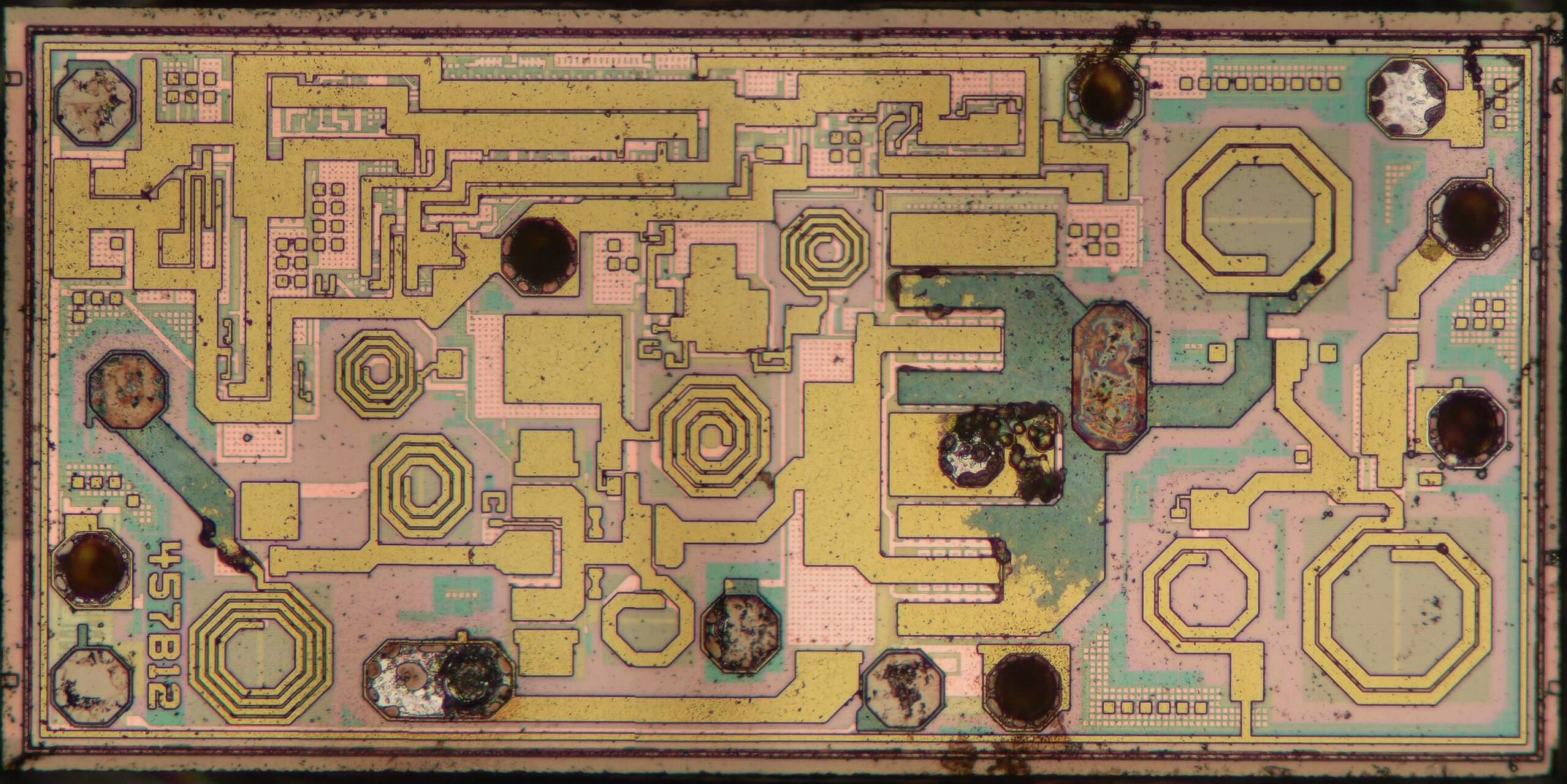
The second wireless chip is slightly easier to figure out. Die #1 is labelled 457B12….
…and die #2 is a 458A01. Neither of these has a manufacturer’s logo or any other markings, but there’s a document floating around the internet that contains both of these codes. There’s no datasheet available, or even any acknowledgement that this product exists other than this document, that describes a manufacturing change affecting several products.
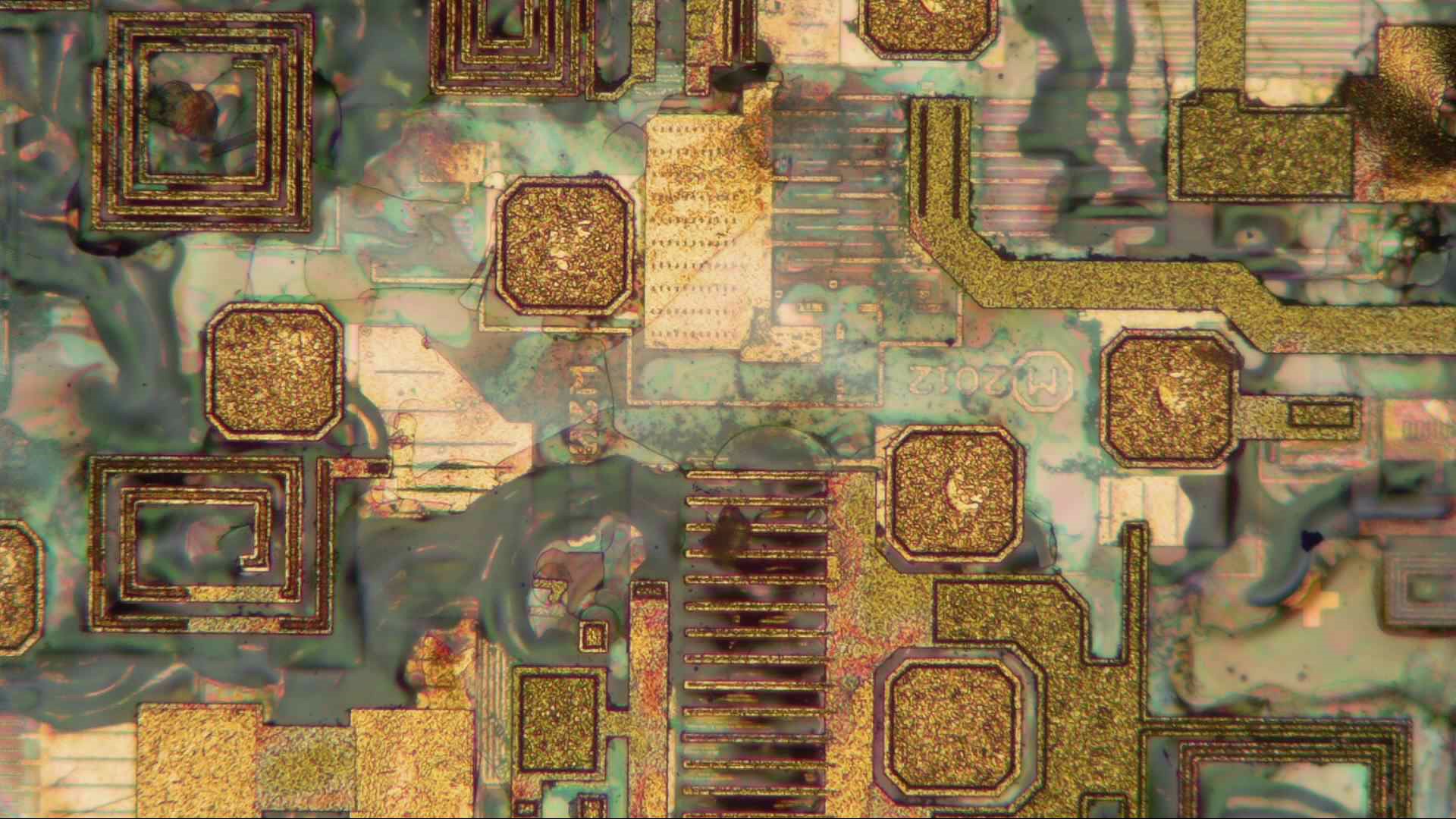
Apparently, these two chips together form a Skyworks SE2618F-07, which is a “2.4GHz 802.11b/g/n WLAN/BT Front End Module with integrated PA, LNA SP3T switch and BT port”. In other words, this is also a front-end module, only for the 2.4 GHz band used by WiFi and Bluetooth. Both dies are made by IBM, die #1 in its 0.35 micron 5PAe SiGeBiCMOS process, and die #2 in its 0.18 micron CSOI7RF process.
Unlike in the 5 GHz FEM, the manufacturer has chosen to implement the LNA and the PA on separate chips. This way, each can be made in a different manufacturing process tailored to its specific function. Die #1 seems to be the PA die, since it has thicker wiring and larger transistors. It also has a very large transistor, just right of the centre, which is probably the antenna switch. You can see a similar device on the 5 GHz chip, just to the lower right of the chip’s centre.
This has become quite a long article, but we’re not done yet! I still have to disassemble the flash chip’s stack and see what’s hiding beneath the main memory die, open up the chips on the bottom of the main board, and have a look at the chips inside the power supply. All of that still to come in Apple TV: Part 2!