The Commodore 64 needs no introduction: an icon of 1980s computing and one of the most-produced computers in history. But successful as the computer itself might have been, its accompanying power supply has always had a reputation for shoddy quality, with many failing even in Commodore’s heyday. If they would just fail by shutting down, that would be one thing, but unfortunately, these PSUs often fail in the worst possible way: by outputting 6 or 7 volts on their +5 V rail, thereby blowing up many hard-to-find chips inside the computer.
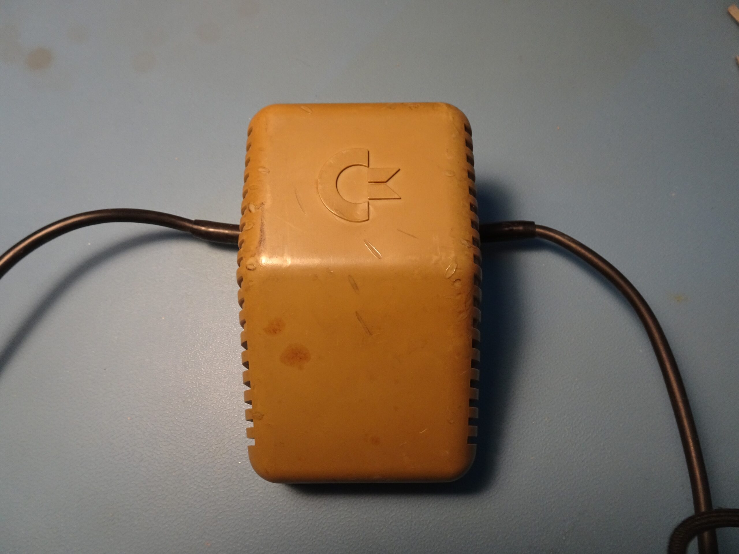
This is the one that came with my C64. It still outputs a neat 5.2 V, but given its reputation I don’t want to risk my Commodore’s guts by using it. Instead, I decided to take it apart and try to improve it. There aren’t any screws on this case, but the bottom eventually comes off if you keep prying on all sides and work it off vertically.
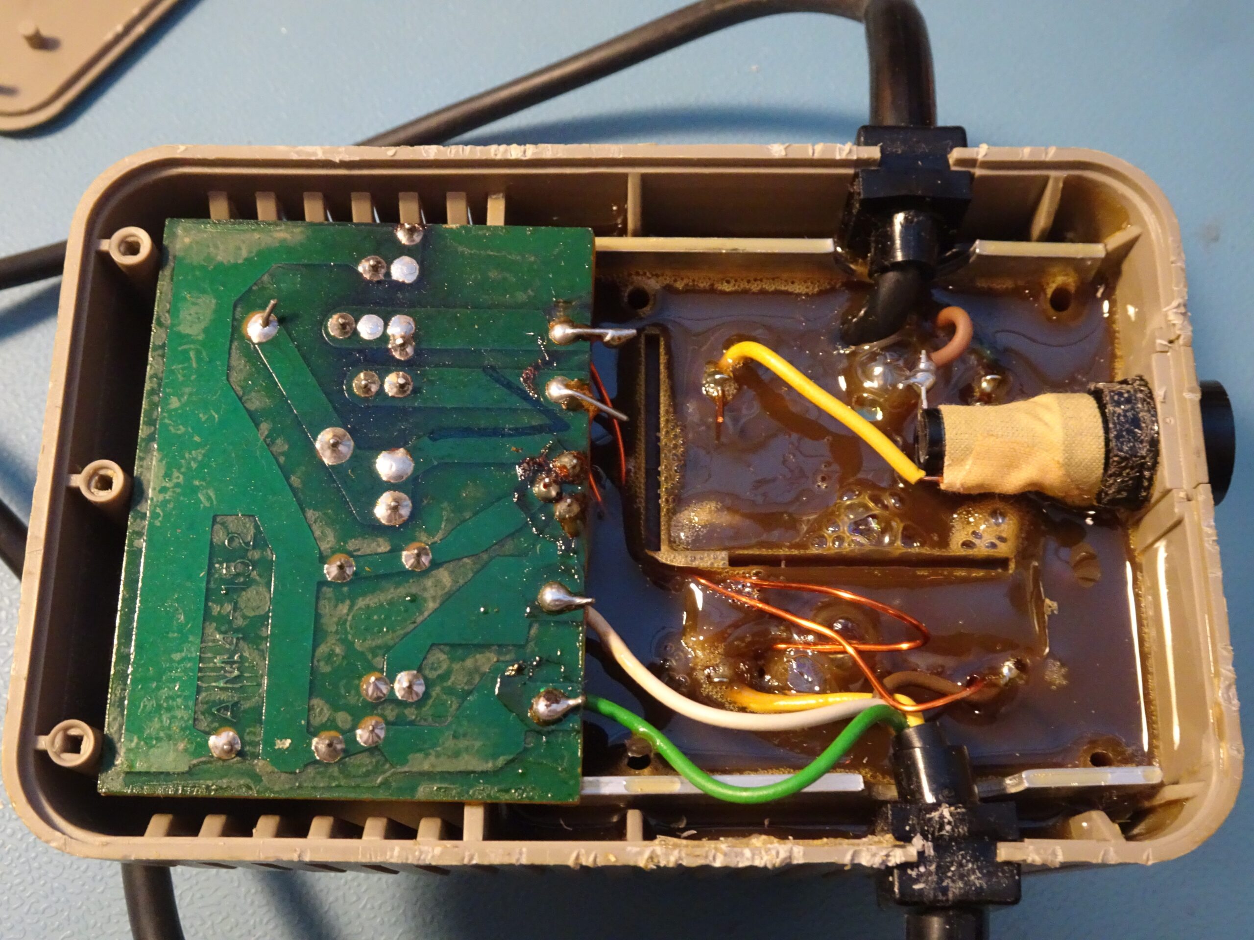
Like most small computers in the 1980s, the Commodore 64 uses a linear power supply. The design is pretty basic: a transformer with two 9 V output windings, of which one goes directly to the computer, and the other connects to the circuit board on the left. The transformer is completely enclosed in potting compound along with the voltage regulator (you can see its three pins in the middle of the board’s right edge).
The voltage regulator gets around 12 V on its input and outputs about 5.2 V on its output. The additional 0.2 V is needed to compensate for the voltage drop along the cable to the computer. For some reason, the designer didn’t use an adjustable regulator like an LM317 but a fixed-voltage 7805, with two resistors to crank up the voltage a little bit. With a 1.5 A rated output current, the 7805 dissipates about 10 W and runs quite hot: this is why the regulator’s body is encapsulated along with the transformer, apparently using the latter’s thermal mass as a heat sink. The whole design is honestly a bit dodgy and it’s not surprising to see a high failure rate.
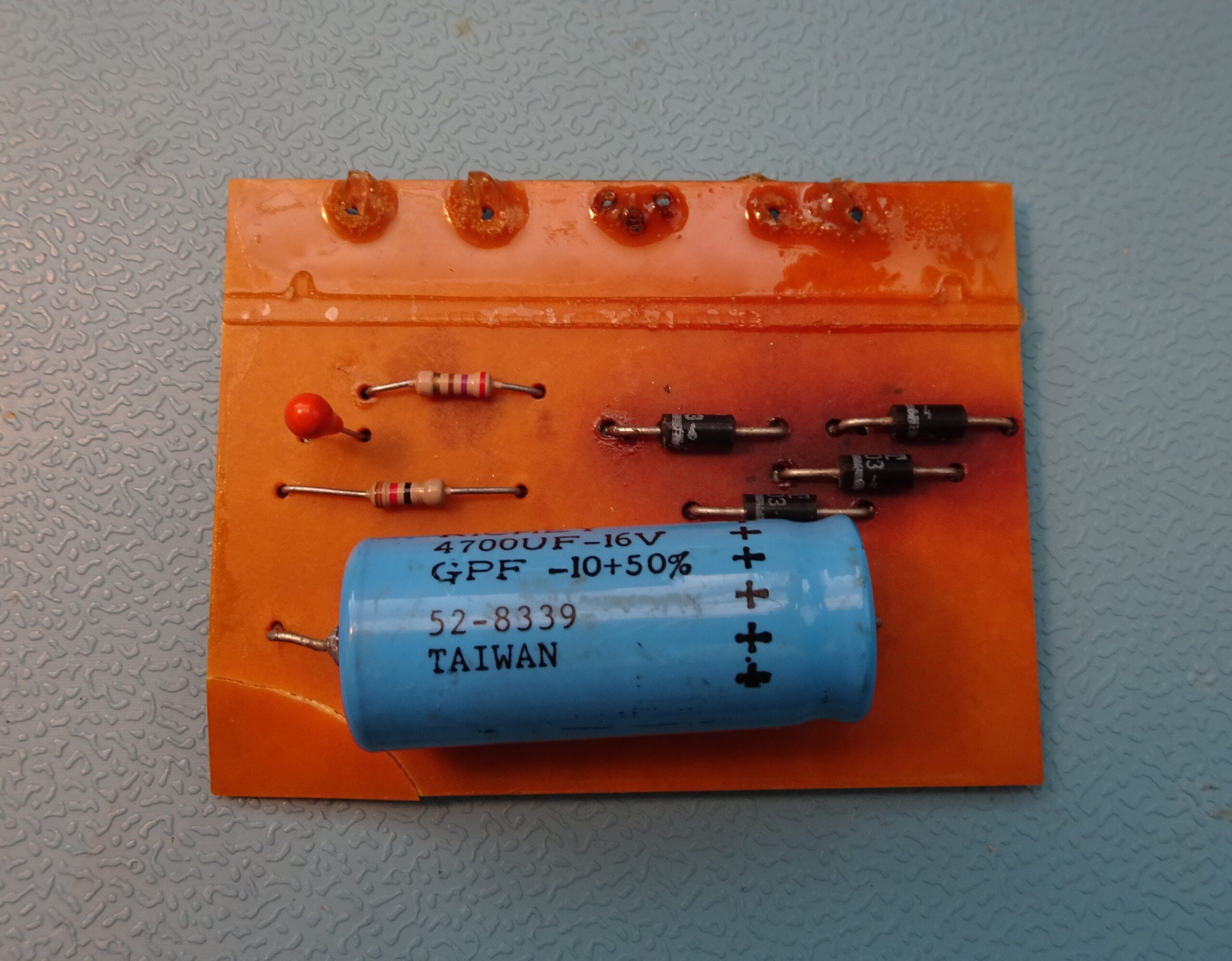
The circuit on the PCB is rather simple, consisting of a diode bridge, a 4700 uF buffer capacitor, the feedback resistors and a 47 uF tantalum output capacitor. The diodes are 1N4003s which have clearly been running hot. This isn’t surprising, because they dissipate almost a watt each due to their 1.1 V forward voltage.
The proper way to tackle all this inefficiency is of course to design a switch-mode power supply instead. Apple famously did so on their Apple II several years before the Commodore 64 was released, but the added complexity and cost meant that most manufacturers stuck to linear power supplies until the early ’90s. Today however, complexity is definitely not an issue anymore because single-chip switch-mode power supplies are widely available. As you can imagine, I’m not the first person to try this, and indeed there’s a wide variety of replacement Commodore power supplies available on the market. But since this blog is about tiny transistors, I decided to set myself a challenge and try to make the new circuit as small as possible.
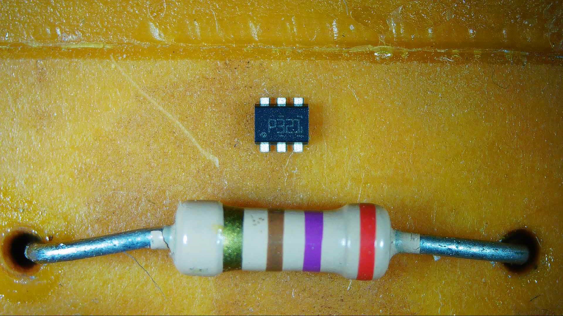
I decided to use the TPS543021 single-chip buck converter, which you can see here sitting next to one of the resistors on the original board. At just 1.6 x 1.6 mm2 it’s definitely a tiny chip, but it can still provide 3 A of output current. That’s twice the rated output current of the original power supply, which is not strictly necessary but might come in handy if I ever use the Commodore with multiple power-hungry peripherals at the same time. It should be able to deliver this extra power without overloading the original transformer, since the original design supplies 10 V times 1.5 A or 15 W to the linear regulator, while the new design outputs 5 V at 3 A, which is also 15 W. The TPS543021’s input draws only slightly more than that since it’s over 90% efficient at full load.
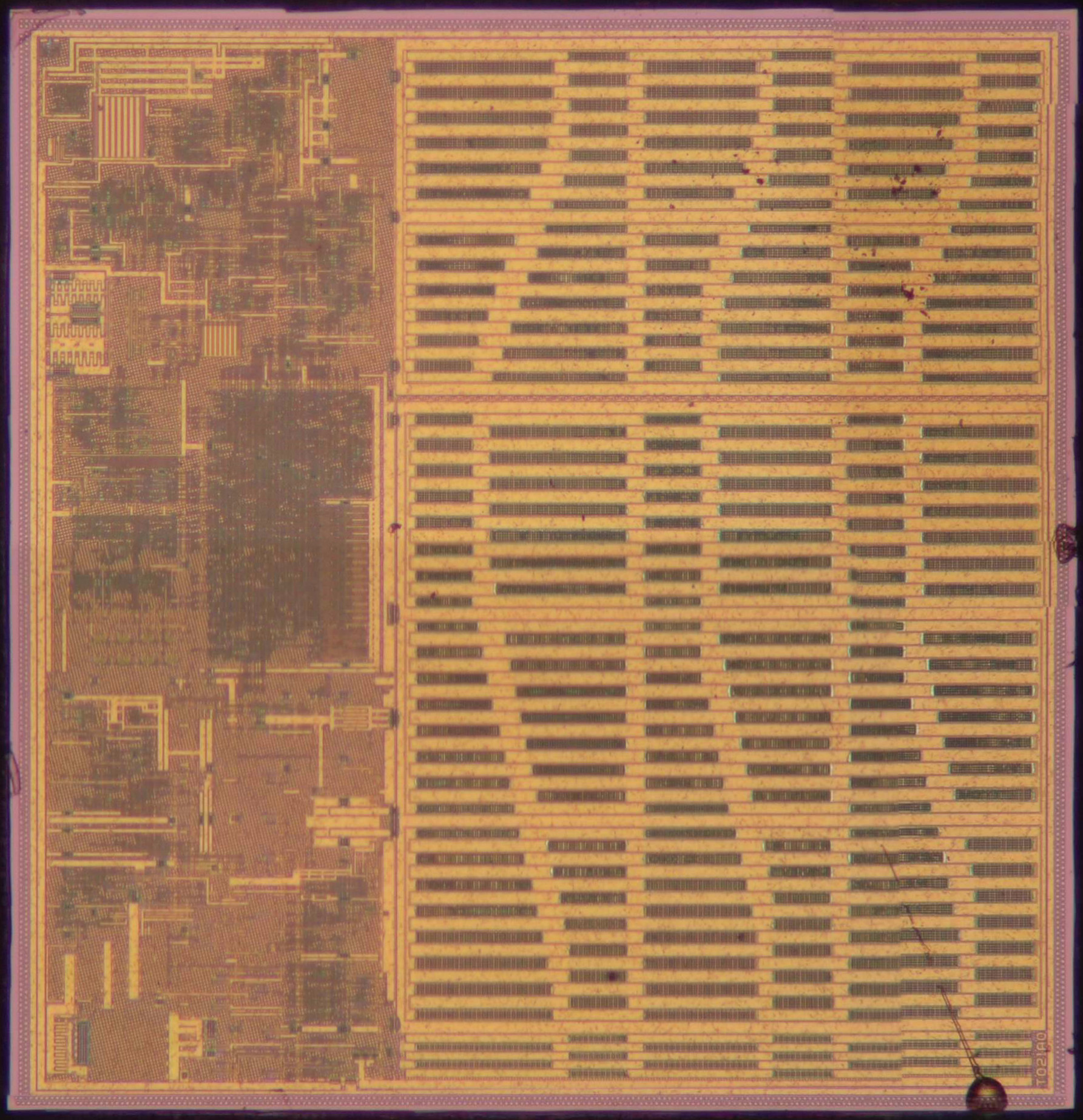
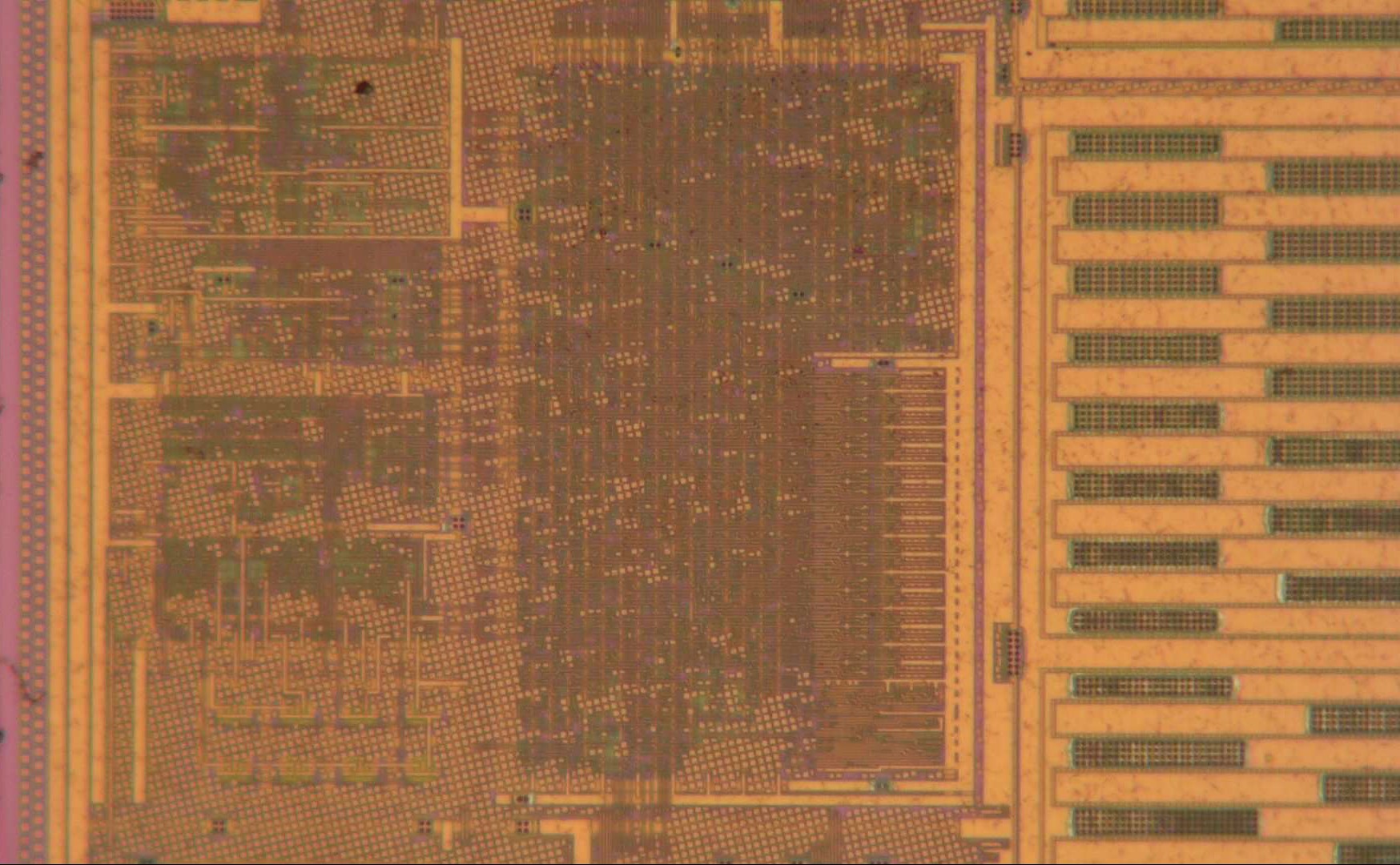
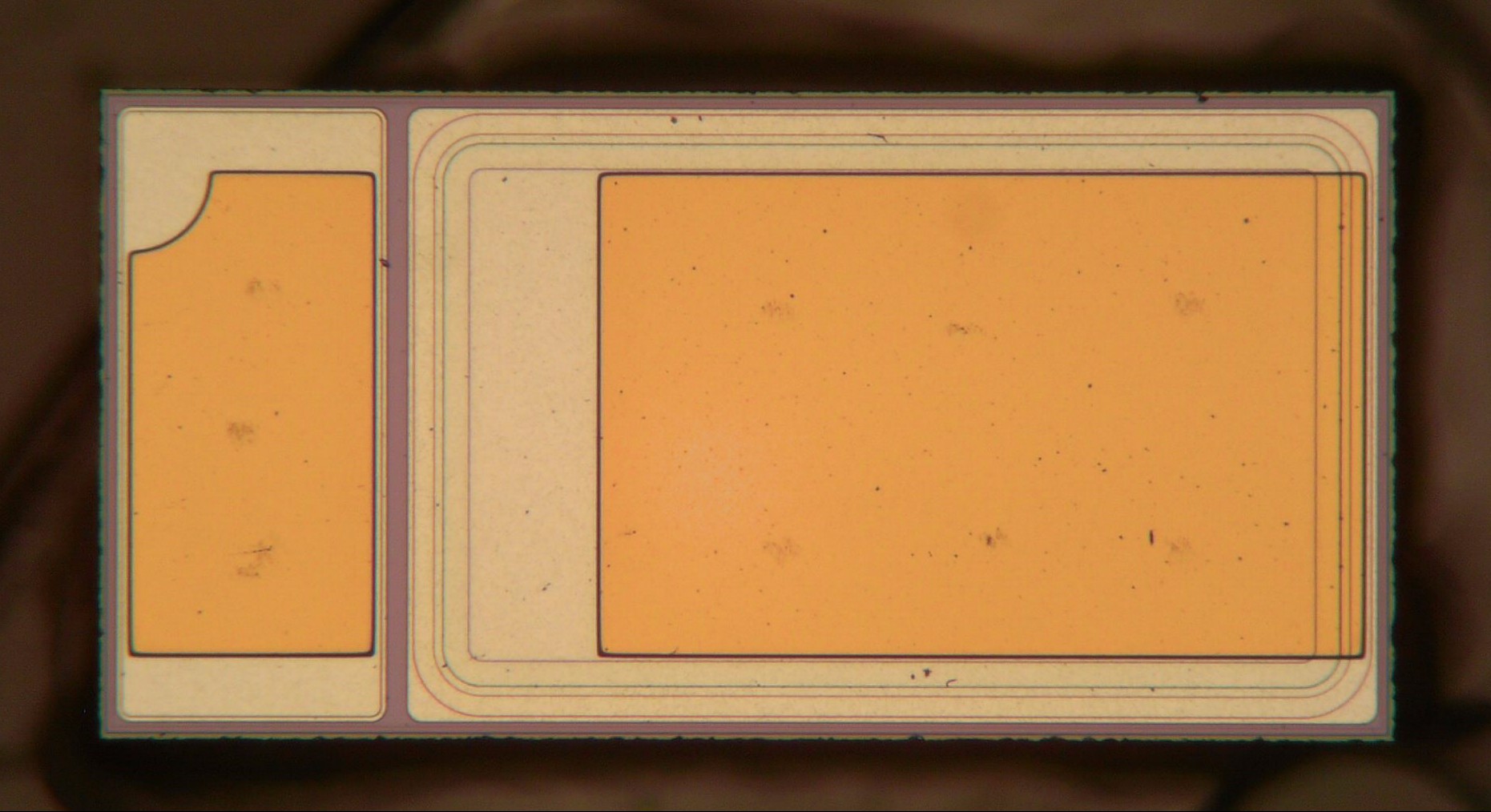
This is what the chip looks like on the inside. The design is dominated by three large power transistors on the right side. Like most modern integrated DC-DC converters, the TPS543021 uses NMOS transistors only. NMOS transistors have a lower on-resistance per square mm than PMOS transistors, so using an NMOS-only design can save significant chip area.
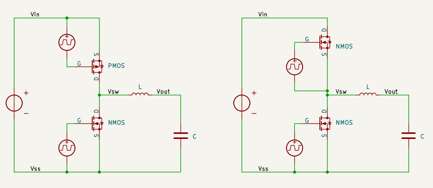
The drawback of using an NMOS for the high-side switch of a buck converter is that it becomes more difficult to drive the gate. MOSFETs only turn on when their gate is higher (NMOS) or lower (PMOS) than their source by at least their threshold voltage. If we use a PMOS for the high-side driver (as shown on the left) we need to drive its gate from Vin down to Vin – Vth, which is easy to do. If we use an NMOS (as shown on the right), we need to drive its gate to Vsw + Vth, because the source of the NMOS is connected to the switching node. And since Vsw moves up and down between Vin and Vss, we need to drive the high-side gate up to Vin + Vth to turn it on fully.
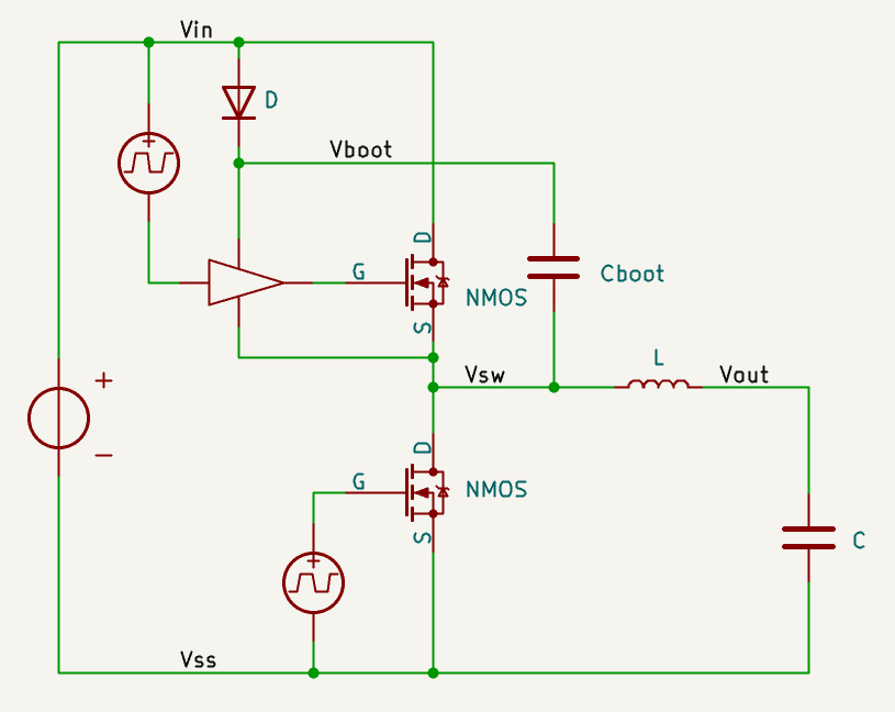
To generate this high-side gate voltage, modern DC/DC converters use a circuit like this, which is known as a bootstrap circuit. When Vsw is pulled low, Vboot is pulled low along with it, causing the diode to charge Vboot to Vin. This is high enough to turn on the high-side switch, because its source is now at Vss. As soon as the high-side switch turns on, it pulls Vsw up to Vin, causing Vboot to be pulled up along with it. This way, the high-side switch pulls up its gate supply “by its own bootstraps”, hence the name of this circuit.
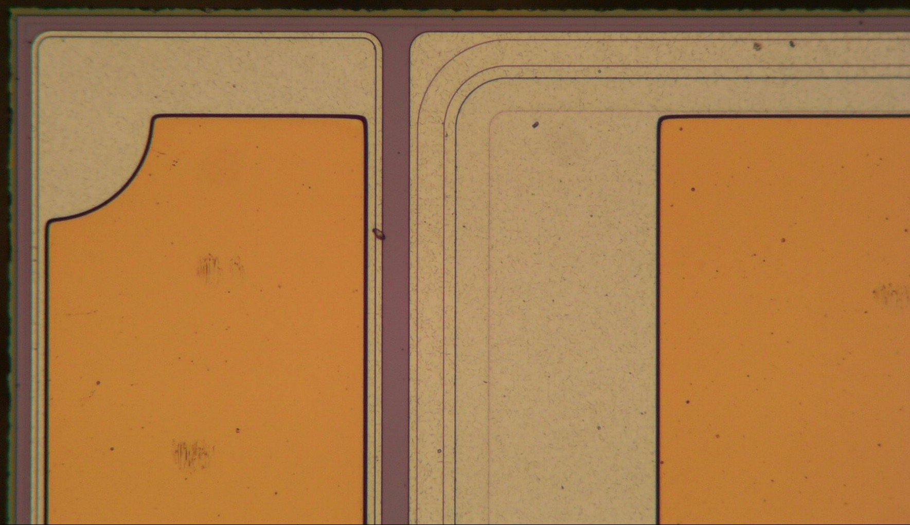
On the TPS543021 die above, we see the diode on the bottom-right, the high-side switch in the middle, and the low-side switch on the top-right.
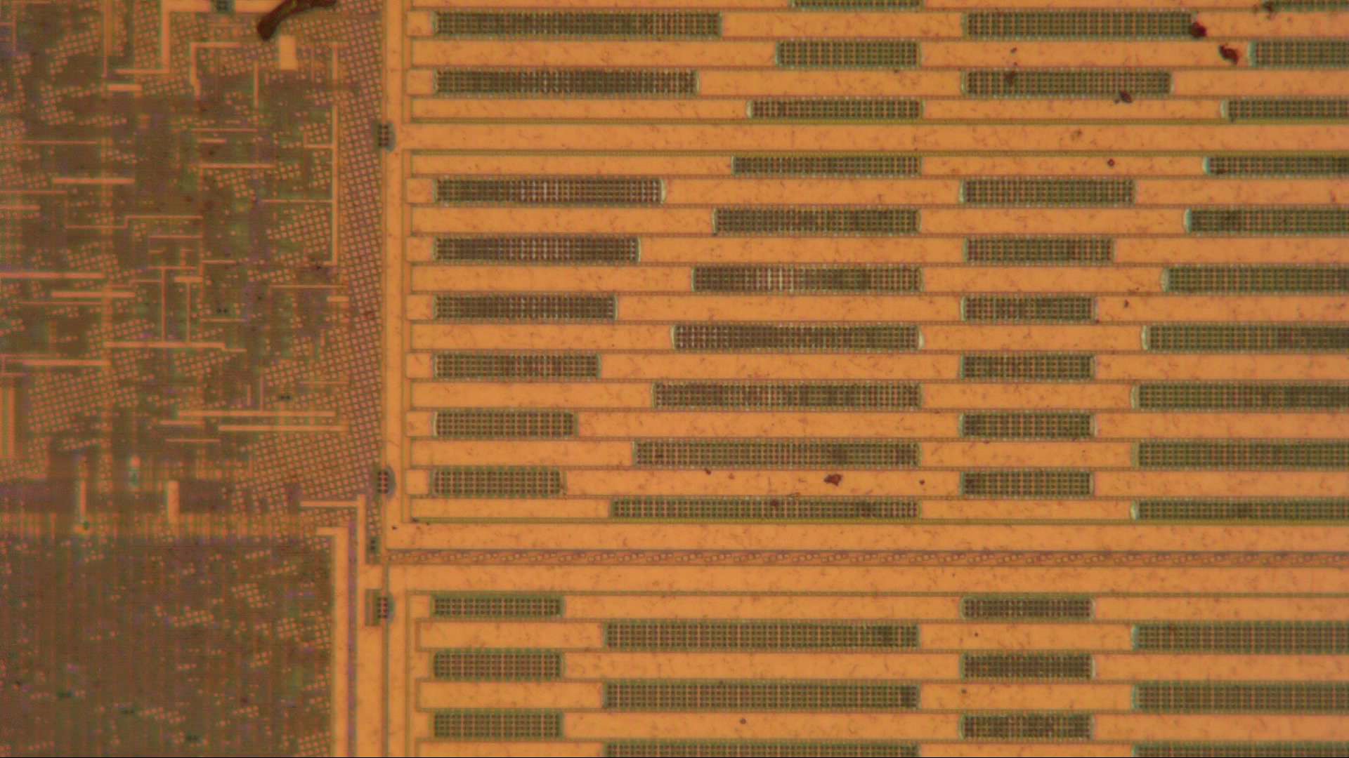
Looking more closely, we can see what the switching transistors look like. The low-side switch takes up the top three-quarters of this image, with a bit of the high-side switch visible below. The dark spotted areas are where the drain and source areas connect to the thick top metal layer, which was etched away along with the package. From left to right, there are alternating columns of drain and source contacts.
The left one-third of the chip contains control circuitry. There’s quite a lot going on over here, because it’s a very sophisticated chip. It monitors the current in the switches, it keeps track of the die temperature, it has a voltage reference, feedback loop control, and a spread-spectrum oscillator.
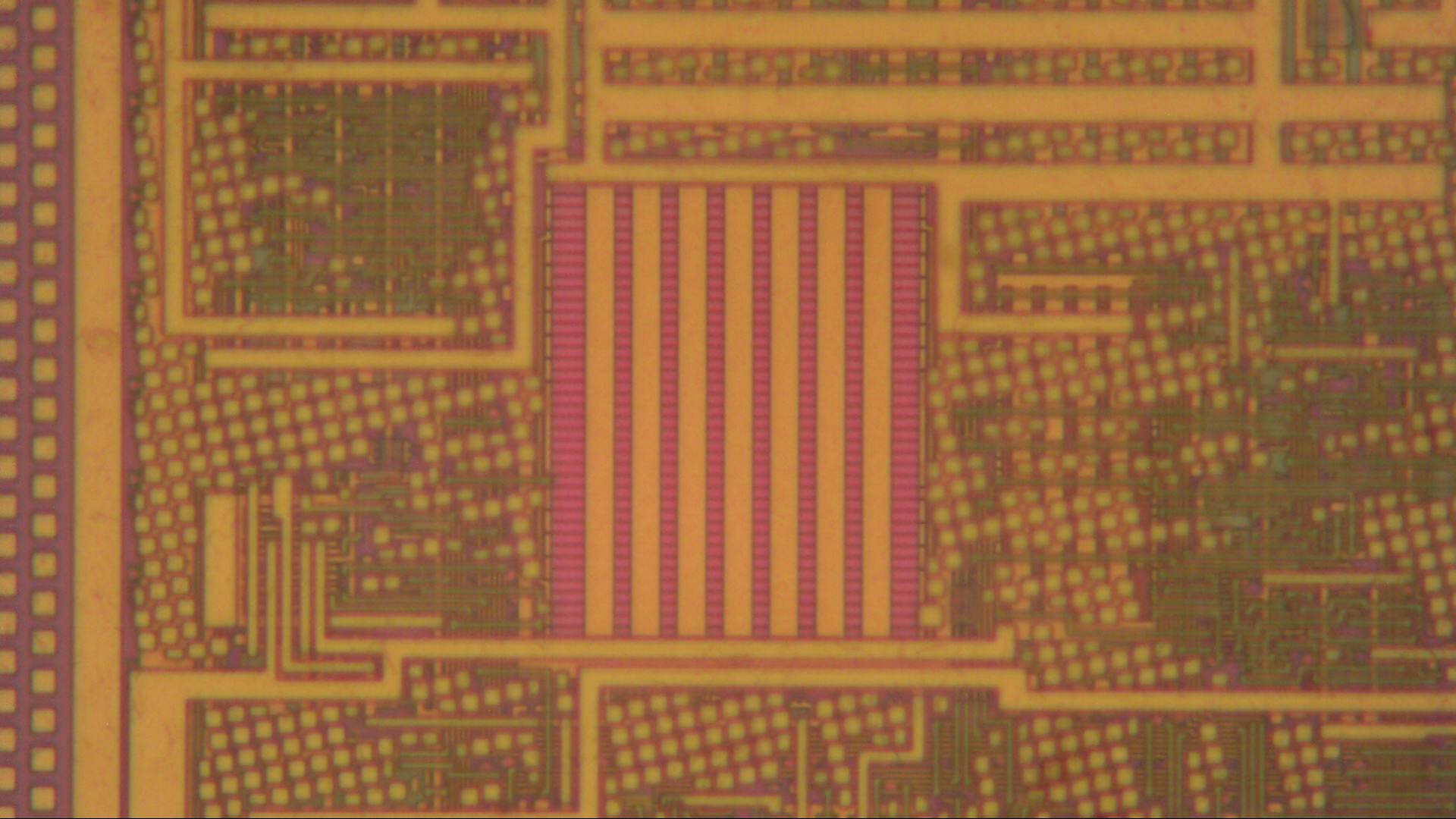
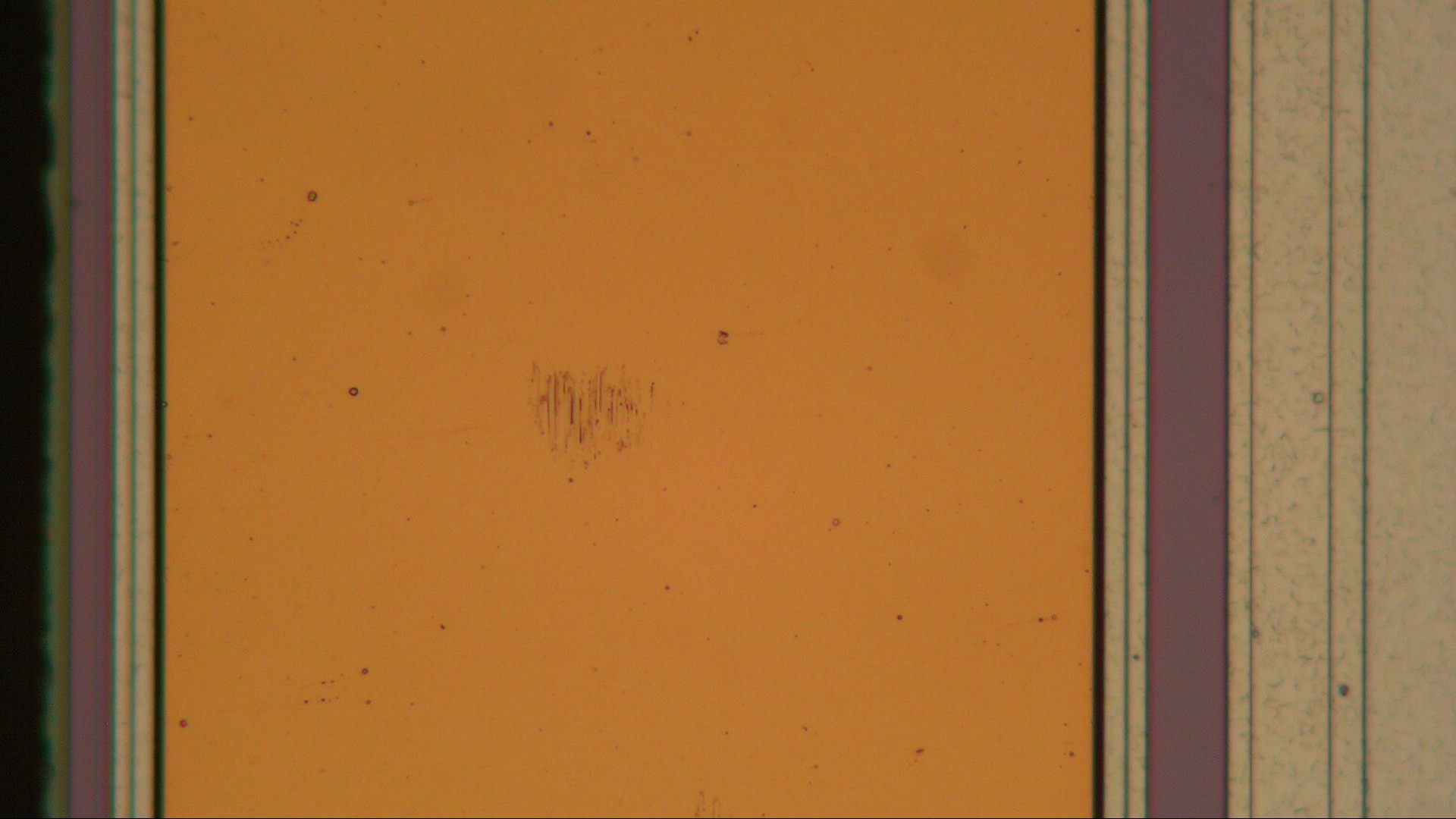
There’s some analog circuitry, as well. Here we’re looking at a meandering resistor chain.
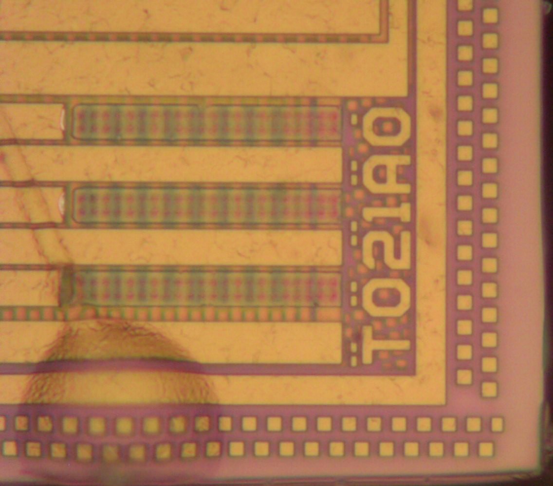
The bottom-right corner has an abbreviated part number. It’s an A0 revision, meaning that the design hasn’t been changed since it was first produced.
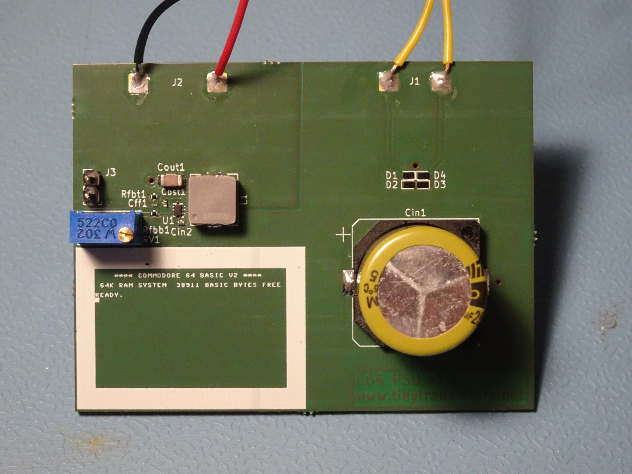
I designed a PCB to house the TPS543021 along with its external components: an inductor, large output capacitor, and a few small resistors and capacitors. The big blue trimpot gives me a bit of trimming range on the output voltage, to compensate for the voltage drop along the power cable, while connector J3 serves to connect a power LED.
On the right we see a diode bridge and a buffer capacitor. Because the switching bit is so small, there’s plenty of space to print a copy of the Commodore’s boot screen.
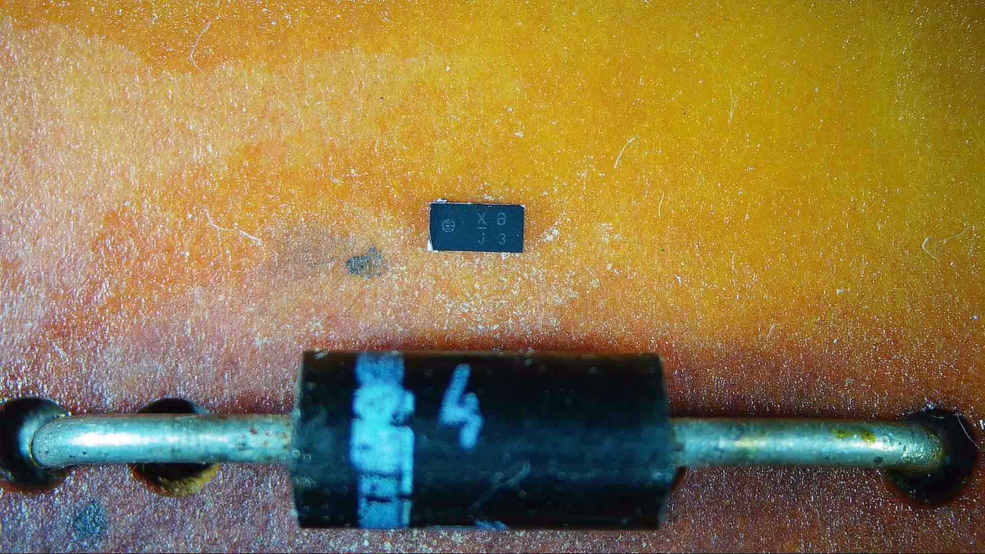
The diode bridge is built from SDM2A40CSP Schottky diodes, made by Diodes Inc. They can block 40 V in reverse and carry 2 A in forward mode, with just a 0.58 V voltage drop. At 1.6 x 0.8 mm2 they’re also much smaller than the original 1N4003s.
The diode is almost a bare die. The back has a thin layer of black epoxy, mostly to block light, but otherwise it’s just a sliver of silicon with two nickel-gold pads for soldering. The lighter coloured metal shapes are aluminium, which is compatible with semiconductor manufacturing but cannot be soldered easily.
The cathode is on the left, which is therefore an ohmic contact. The Schottky junction is below the anode on the right. We see rounded rectangle shapes which help to avoid high field strengths in the corners of the junction.
In fact, it looks like there are several rounded layers below the anode contact. Although the basic idea of a Schottky diode is simply a metal contacting a semiconductor, an actual device apparently contains several other layers.
Several locations on both the anode and cathode show these scratch marks. These are left by the automated test equipment (ATE), which tests every single device by probing the pads with sharp needles and measuring the electrical characteristics.
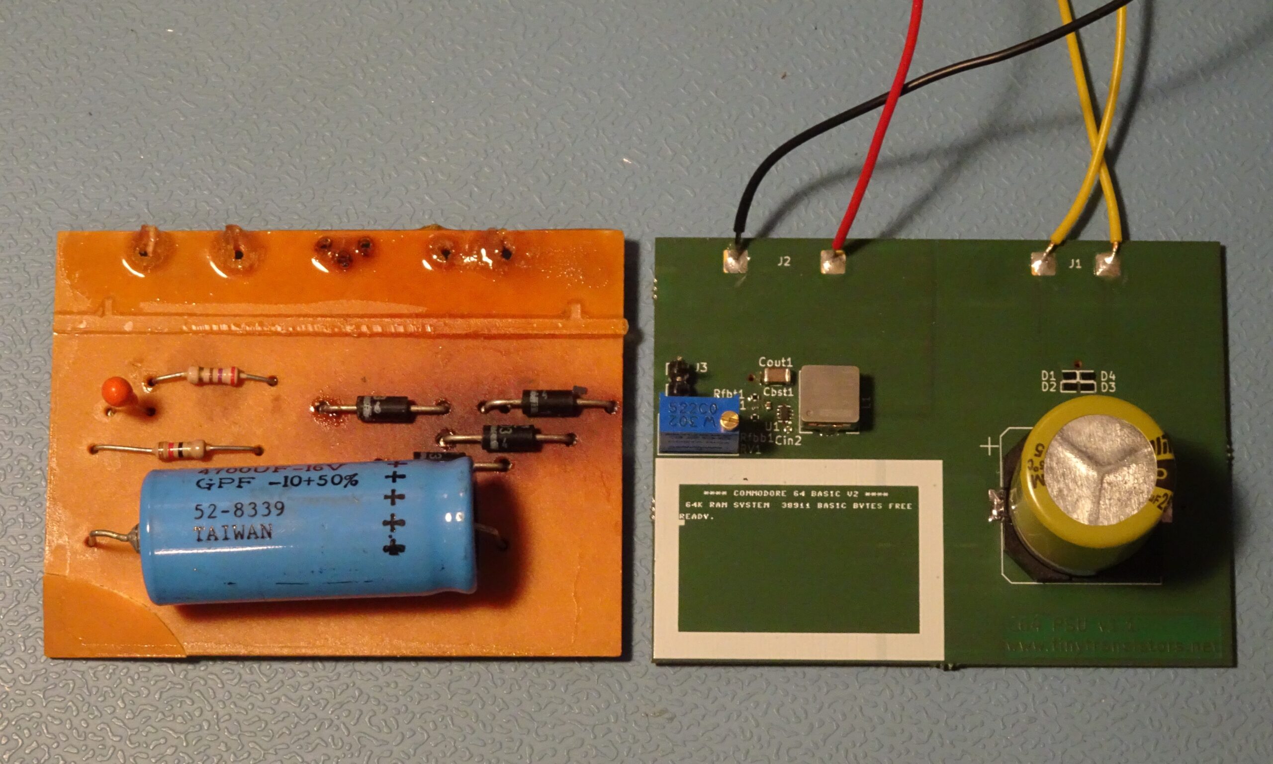
Here are the old and new board side by side. Like the old board, the new one has a 4700 uF buffer cap, which is still the largest component by far. Nevertheless, forty years of technological development has about halved its volume.
I hooked up the finished board to a lab PSU and an electronic load to test its performance. I adjusted the trimpot to get around 5.2 V on the output.
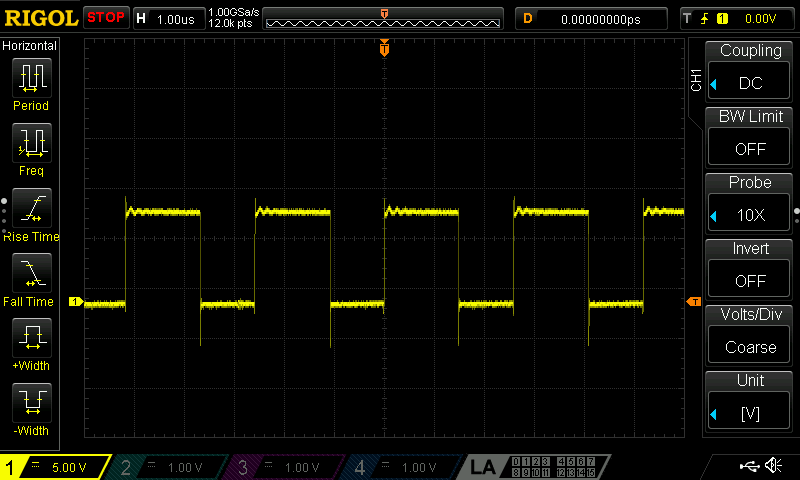
At light loads, 200 mA in this case, this is what the switch node looks like. The converter is operating in discontinuous mode.
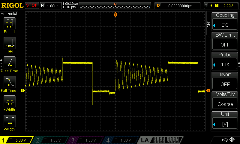
At higher loads (800 mA) it switches to continuous mode. This is what we see on a single sweep.
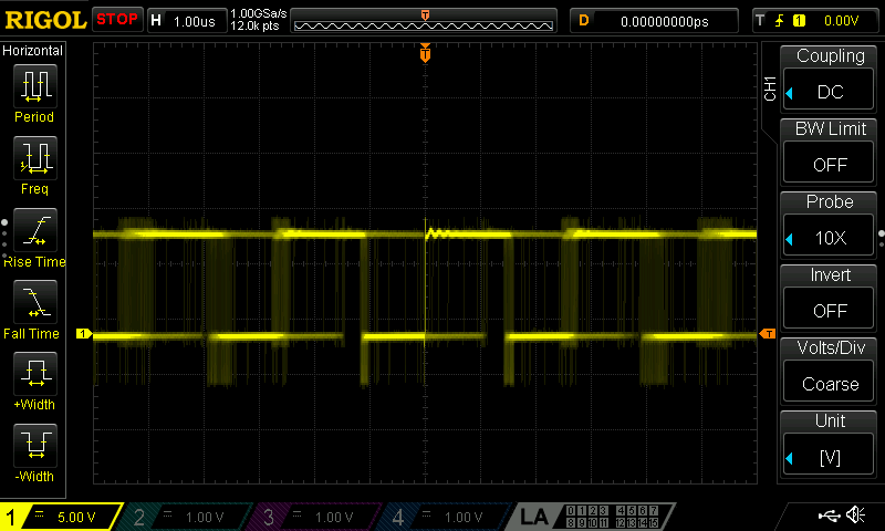
If we look at the screen continuously however, we see that the frequency is changing all the time. This is the spread spectrum technique that it uses to minimise electromagnetic interference.
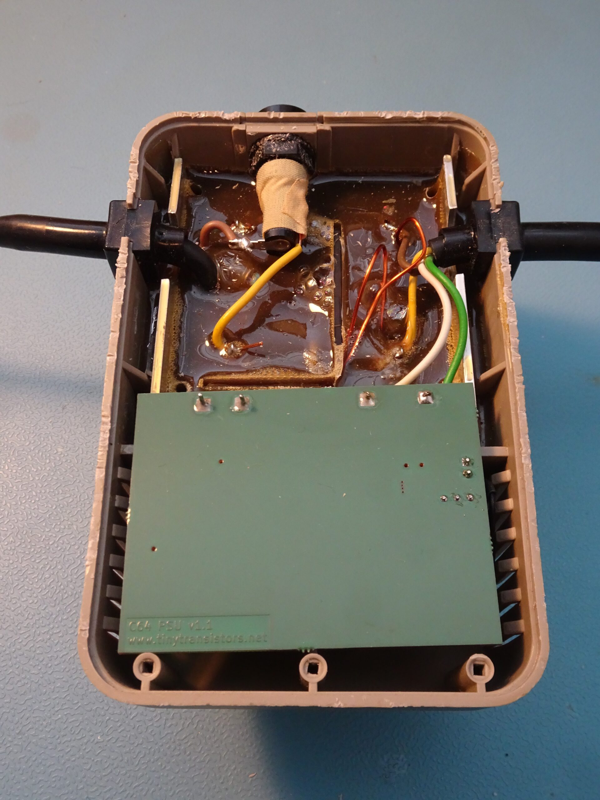
Here’s the new board inside the original power supply. I also hot-glued a red LED to the inside of the slotted part of the case.
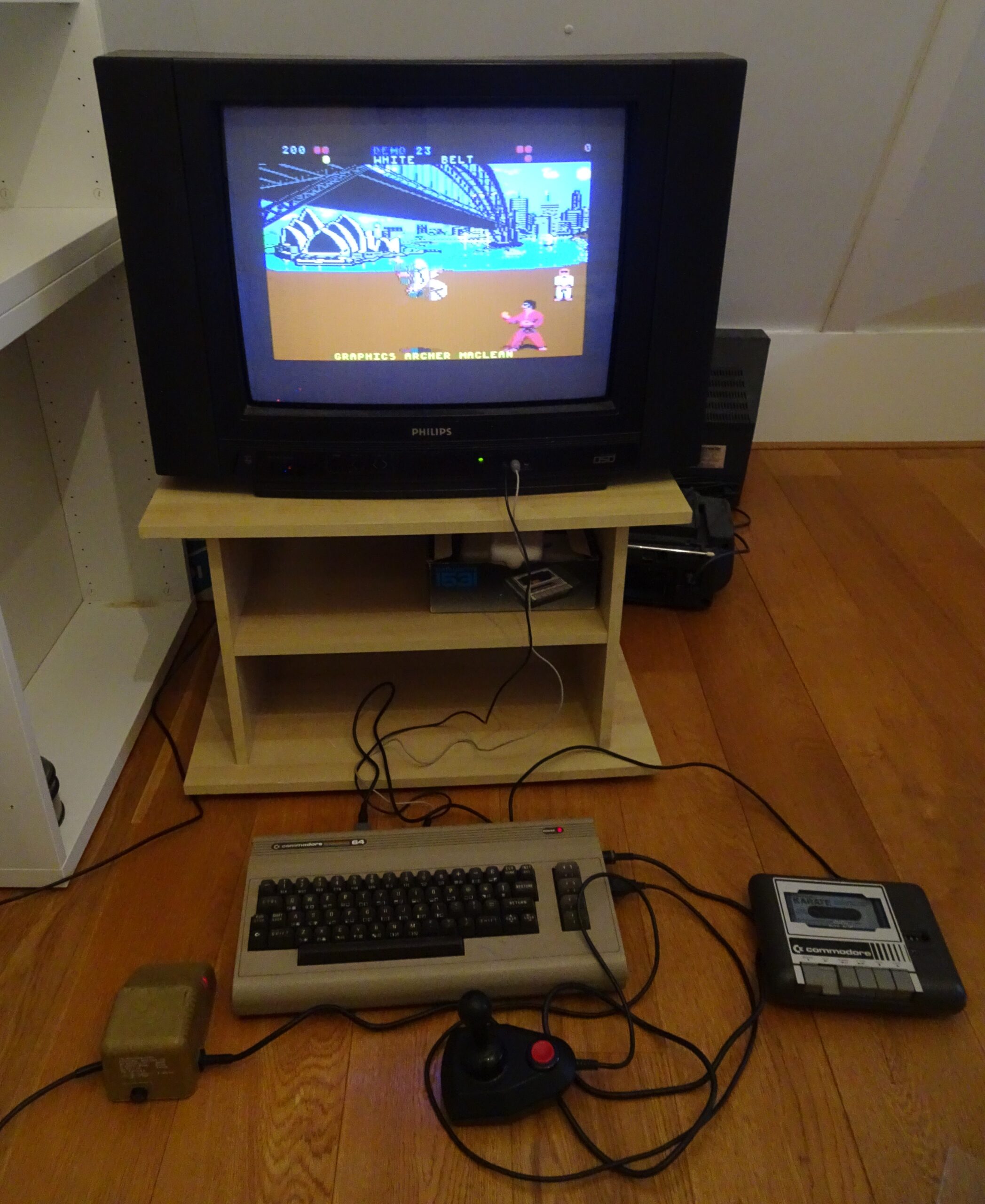
And here’s the revamped PSU powering my Commodore 64, along with the 1531 Datassette. It’s loaded International Karate and seems to be working perfectly well, ready for the next forty years!